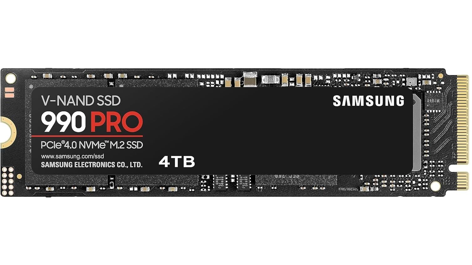
At one point in time, it was the fastest PCIe Gen 4 drive you could buy. Now, the next generation of PCIe 5.0 drives is available, but the 4TB Samsung 990 Pro still offers extremely fast performance and whopping amounts of capacity in a single-sided M.2 2280 form factor. The main issue at the moment is price. Thanks to the AI boom driving up the prices of memory and storage, SSDs have reached insane highs, so to be able to take advantage of a large 27% discount in these times is nothing to be sniffed at. The 4TB Samsung 990 Pro has fallen from $1,099 to this new price of $799.90, a saving of over $300. This works out as roughly 20 cents per Gigabyte of storage capacity.
Having reviewed the Samsung 990 Pro 4TB when it was released, we found it to be one of the best 4TB SSDs on the market and among the best SSDs overall. The 990 Pro boasts maximum sequential reads of 7,450 MB/s and sequential writes of 6,900 MB/s, with random reads/writes coming in at 1.6 million and 1.55 million IOPS, respectively, while endurance is rated for 2,400 TBW.
990 Pro 4TB SSD: was $1099.99 now $799.90 The Samsung 990 Pro 4TB is among the fastest Gen 4 SSDs available thanks to read and write speeds of up to 7450/6900 MB/s, almost maxing out the Gen 4 bandwidth. This M.2 NVMe drive comes in the 2280 form factor and holds enough capacity to store a large selection of your favorite games or files.
Random reads/writes come in at 1.6 million and 1.55 million IOPS, respectively, while endurance is rated for a respectable 2,400 TBW.View Deal
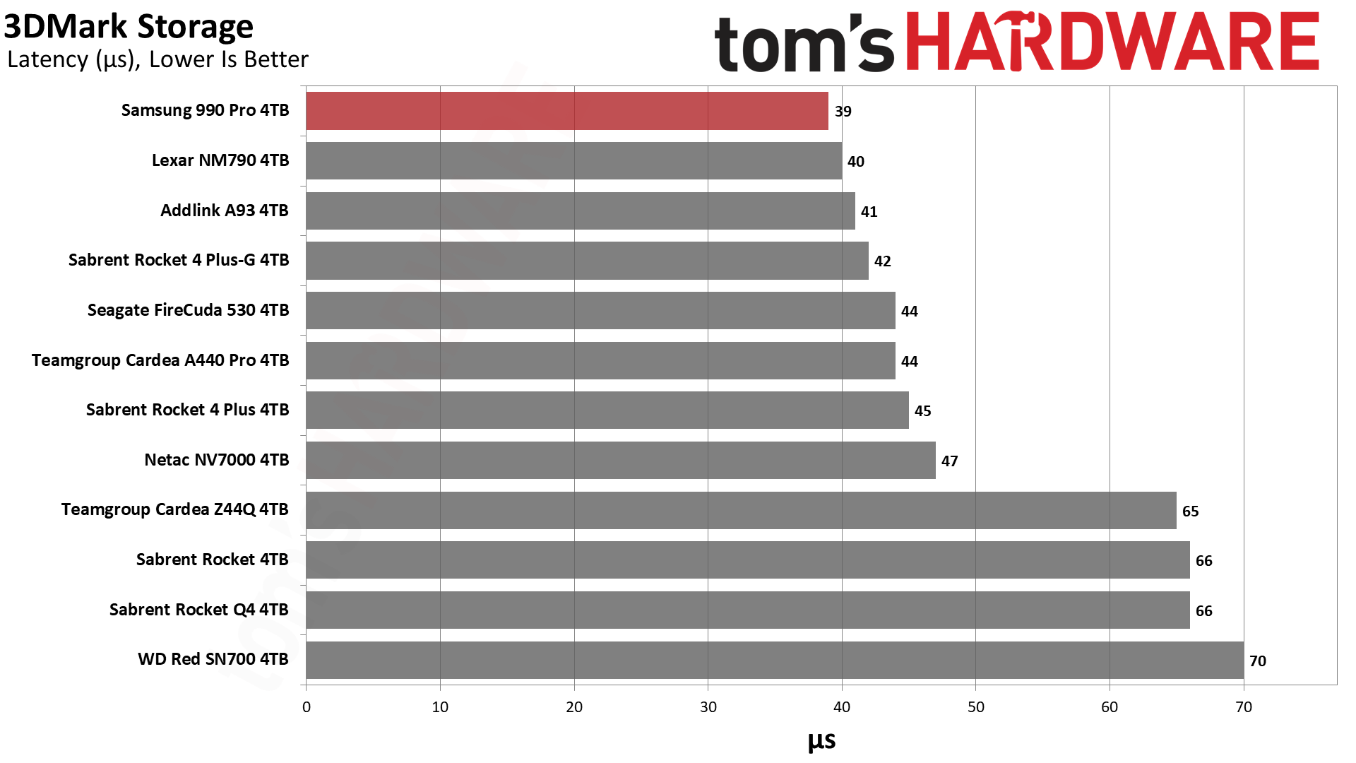
Samsung uses 236-layer TLC V-NAND to achieve its 4TB capacity, while also using a single-sided design, making the 990 Pro ideal for use in computers where space is a finite resource. When we tested the Samsung 990 Pro 4TB, we found it scored above the competition on almost every test. On 3DMark's storage test, it had the lowest latency result, a big plus for responsive load times in gaming.
(Image credit: Tom's Hardware)
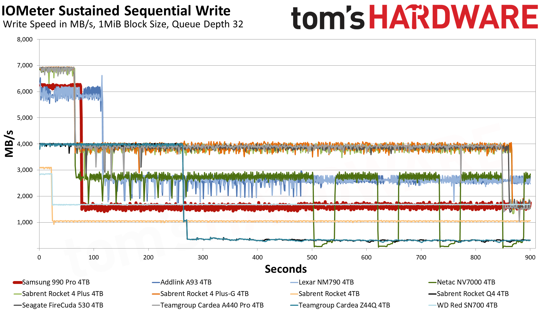
The Samsung 990 Pro is also excellent at sustaining strong write performance. In our IOMeter sustained sequential write tests, the 4TB 990 Pro was able to maintain a speed of 6.2 GB/s for 75 seconds thanks to its generous 10GB of pSLC cache. Once the data spills over into the TLC, it operates at 1.6 GB/s. The Samsung 990 Pro is also a leader in power efficiency, delivering 421.1 MB/s per watt. That number puts it ahead of all competitors but the Addlink A93 4TB and Lexar NM790 4TB.
(Image credit: Tom's Hardware)
The Samsung 990 Pro is certainly nowhere near the all-time low prices of years gone by, and I'm not sure at the moment when, if at all, we'll ever see those low prices again on storage, certainly not for some considerable time. If you want 4TB of storage now, then the Samsung 990 Pro is a formidable choice; just try to grab it when there's as much of a discount as possible.
SSD controller designer FADU’s new File-Semantic SSD (FS-SSD) was announced at the 2026 OCP Global Summit. The new device promises to move the file system into the SSD itself. As detailed in a white paper, this enables GPUs, DPUs, and NICs to open and read files with “no host filesystem, no block layer, and no storage-server CPU in the path.” FADU told Tom’s Hardware Premium it expects partner samples by Q3 2027.
FADU is a Seoul, South Korea-based fabless SSD controller designer. Its FS-SSD technology is designed to handle and improve the control path, as the data path side moved to accelerators years ago. FADU’s measurements show that the file system, plus block layers, can consume about 30% of CPU cycles in a GPUDirect Storage (GDS) random-read workload. It notes that bypass options give up the files, and the company claims its solution promises the best of both worlds.
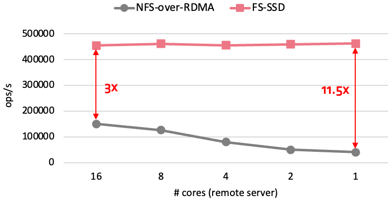
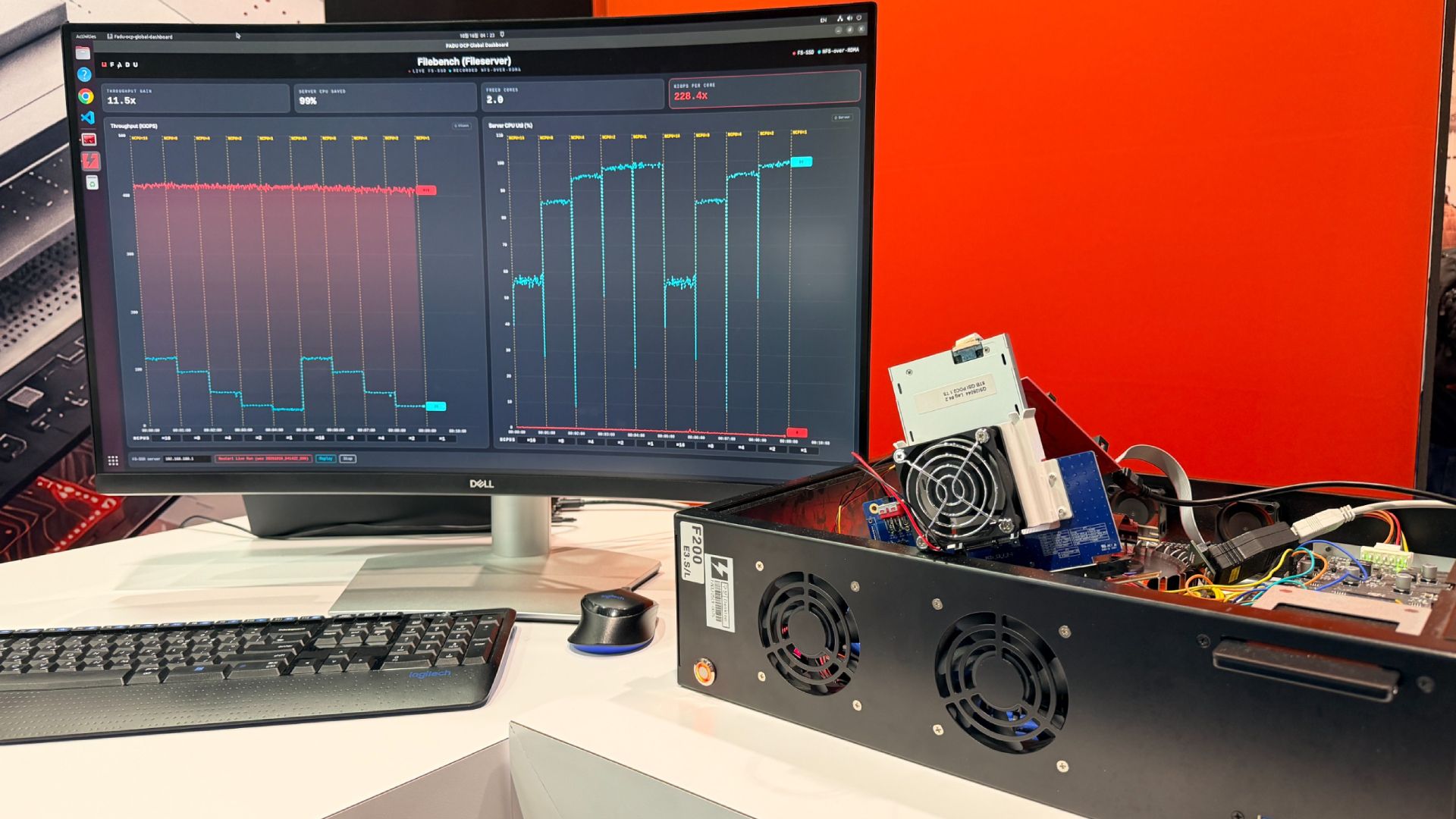
In FADU’s own preliminary Network File System (NFS) over NVMe test, on a drive built on its FC6161 Gen6 controller in a PCIe 5.0 host, remote file throughput held steady as the server downshifted from what FADU labels 16 cores to just one, maintaining about 460,000 ops/s.
The NFSv3 operations are carried inside standard NVMe commands, and the drive handles path lookup, access control, and file-to-flash mapping. FS-SSD’s performance is remarkable when compared to Linux NFS-over-RDMA, which achieved a third of the ops/s with 16 cores and only 40K ops/s with one core. The technology remains “under active development,” and FADU told Tom’s Hardware Premium it expects Gen6-host results by Q1 2027, with partner samples in Q3 2027.
FS-SSD holds about 460,000 ops/s from 16 server cores down to one, while NFS over RDMA falls from approximately 150,000 to 40,000 ops/s (Image credit: FADU)
FADU chooses to use NFSv3 because it’s “small (21 operations), OS- and filesystem-agnostic, and stateless” with low firmware overhead. FS-SSD supports PCIe today, with NVMe-oF over RDMA and TCP working without any new transport needed. Reusing an existing protocol is a smart move, in our view. Under the hood, the file system and flash translation layer are merged with a file layer derived from F2FS. Node and data blocks are aligned with the natural flash pages, sections at corresponding erase units, so that the F2FS node table becomes a “File Map” pointing the node IDs at physical flash addresses.
One big advantage is that the DRAM mapping metadata overhead is considerably smaller: it uses the same amount of DRAM as a standard SSD, ~0.1% of NAND capacity (about 1 GB per TB), which a standard SSD fills almost entirely with its mapping table. Here, most of that DRAM, ~95%, can act as a hot-path node cache.
One garbage collector also replaces two, avoiding what FADU calls the “double GC” of host F2FS, where file-system cleanup and the drive’s own garbage collection amplify each other. Write amplification is also 63% lower versus a host F2FS solution on a mixed sequential and random workload with FADU’s research prototype, the company said. FADU told Tom's Hardware Premium that the prototype runs synthetic fio workloads on NVMeVirt, an open-source software SSD emulator from Seoul National University, so it is not a hardware result.
Most importantly for this method, it ensures host-free access. The GPU builds NFS-over-NVMe commands in queues in its own memory, which could include HBM. Alternatively, a remote SmartNIC or DPU with NVMe-oF target offload can drop commands in the drive’s submission queue. The data goes from SSD to NIC via PCIe peer-to-peer DMA, coming out as RDMA writes. FADU’s explicitly named use cases for this include GPU file reads and checkpoints, DPU-served HTTP content delivery, and a JBoF (just a bunch of flash) file server.
FADU’s numbers for its internal test come from a client and server Intel Core i5-13600K, a CPU with 20 threads that clocks up to 5.1 GHz with 128GB of DDR5, and a Mellanox ConnectX-6 100 Gbps NIC. Synthetic testing is compared using fio with the baseline F2FS and Ext4 on block firmware versus the FS-SSD via a kernel client and an SPDK user-space client. The sequential test is 1 thread, queue depth (QD) 128, with 128KB blocks, while random is at 4 threads, the same QD128, but with 4KB blocks.
These block sizes are typical for client workloads in our experience, so they are a fair measure, with detailed preliminary results in the table below. Against SPDK on the raw drive, figures FADU provided to us, FS-SSD’s SPDK client keeps about 93% on 4K random read and 53% on 4K random write, via fio, with around a 7% and 47% cost for the in-drive file layer. Though the raw drive’s 13,240 MB/s random write is above the ~12 GB/s FADU gives as the NAND’s program bandwidth, those runs likely weren’t at steady state. The Filebench result is particularly interesting, as the SPDK random gains apply to a plain block device too.
This should be the workload most favorable for the technology, as the Filebench file server is metadata-heavy with relatively high host overhead: FADU says it uses 10,000 files in a multi-level tree, mean directory width 20, and a mean file size of 128KB with 50 client threads.
FADU’s preliminary fio results: Gen6 controller in a PCIe 5.0 host, direct I/O
Setup
Sequential read (MB/s)
Sequential write (MB/s)
4KB random read (MB/s)
4KB random write (MB/s)
F2FS
14,120
4,510
7,850
3,980
Ext4
14,130
7,050
9,120
4,560
FS-SSD (kernel client)
14,140
11,940
8,070
4,320
FS-SSD (SPDK client)
Not reported
Not reported
13,000
7,030
Raw block (SPDK)
Not reported
Not reported
13,990
13,240
One important thing to recall is that although this test is on a Gen6 drive, the test results are on a PCIe 5.0 host. Therefore, every sequential read config tops out at around 14.1 GB/s, which is roughly the link limit. The testbed also uses a consumer-class desktop CPU, while the one-core NFS server is a showcase example. The kernel client ends up 11.5% behind Ext4 on random read and 5.3% behind on random write, again by our math.
One example of a tough question more generally is: how do concurrent GPU, DPU, and host writers coordinate? How does a kernel mount’s page cache stay coherent with GPU access? NFSv3 storage devices, by the pNFS Flexible File Layout spec (RFC 8435), are “always treated as loosely coupled,” which means “Mandatory byte-range locking cannot be supported.”
Credentials riding in the NVMe command may also face security issues, as loosely coupled devices get only “a level of security equivalent to AUTH_SYS,” NFS’s basic scheme, in which the server trusts whatever user and group IDs the client sends. FADU’s published material also does not describe features such as snapshots, encryption handling, quotas, ACLs, crash handling, and so forth, related to this. Statelessness is what makes it work, but it doesn’t solve all problems, so the trust factor moves elsewhere.
In reply to our questioning, FADU said that there is no cross-host locking, as NFS’s lock manager isn’t implemented. The drive applies each write whole, in order. If two writes hit the same spot, the second one wins; this is “last-writer-wins.” Coordination depends on the clients: kernel-mounted ones get the usual advisory locks among themselves, GPU and SPDK clients coordinate in the application, and at scale a pNFS metadata server handles the coordination. Caching is also handled like ordinary NFS, with kernel clients, or is not done at all, for GPU and SPDK clients. This is stock NFSv3 behavior.
The drive has to check user/group IDs against the file permissions itself. Because those IDs ride inside the command, a client could fake them, but FADU says it closes that issue with capability-based authentication. Each command carries a capability issued by an outside authentication server, plus a code computed with a key shared only between that server and the drive. This is not detailed in its published material. FADU adds that support for the Kerberos authentication protocol is planned. For networked drives, the standard NVMe-oF protections are used, with only pre-approved hosts admitted. A drive trusts a single host’s kernel like any NVMe drive.
However, as FADU described to us, ACLs and other features are missing in the current release, aside from encryption, which in this case is handled by the FC6161’s standard TCG Opal self-encrypting drive support. Power loss is also typically handled with capacitors flushing metadata, the write buffer, and a log of in-flight operations. On restart, the drive replays the unfinished operations, and every write is durable if the drive acknowledges it.
FADU’s longer sights are on producing a JBoF storage solution with no server in front: FS-SSDs, a PCIe switch, and a DPU or NIC for handling NVMe-oF in hardware. FADU’s model puts this at about 42% lower power, about 57% lower cost per 16-drive server, and higher rack density with significantly lower five-year total cost of ownership. The drives would slot in behind existing pNFS metadata servers and could scale. FADU’s controllers already ship with drives such as the SN861, which Western Digital launched and SanDisk now sells, but this would expand the options and solutions it can provide.
FADU’s FS-SSD roadmap
Milestone
Timing (per FADU)
Details
Gen6-host results
By Q1 2027
FS-SSD tested in a PCIe 6.0 host; hardware write-amplification figures to come with them
Partner samples
Q3 2027
OEM/ODM talks are at an early stage; active collaboration expected once samples ship
Hostless JBoF
By end of 2027
Reference design built on Xsight Labs E1 DPUs, delivered to OEM/ODM partners
GPU access
Now, via GPUDirect Storage
Works with GDS through the kernel client; FADU intends to join the Accelerated IO SIG (xio-sig), where Nvidia open-sourced cuFile; no direct engagement with Nvidia
Standards
Nothing submitted yet
FADU plans to start a file-semantic command set discussion at NVM Express and OCP Storage; samples and client code come first
Next year should bring real numbers and samples, with the JBoF reference design also expected. There may be an NVM Express or OCP Storage proposal down the line for a file-semantic command set to further cement and mature the approach. FADU has a good idea, is building it on an existing framework, and has a testbed with results and a hardware path forward on its Gen6 controller, with a trust model in mind. A Gen6-host run is now needed to support the company’s claims.
Intel and AMD are integrating their CPU optimizations for PyTorch into a unified library, offering tuning for both AMD and Intel chips through the oneDNN library. AMD has maintained a downstream version of oneDNN called ZenDNN, which is now moving into the open-source oneDNN, published by the UXL Foundation and driven by Intel. AMD also announced it's joining the UXL Foundation as a "steering member," which "influences the future of the UXL Foundation" in exchange for a contribution of $20,000 per year.
AMD says the move to unify these efforts under oneDNN was recommended by the x86 Ecosystem Advisory Group (EAG), which is a joint initiative that primarily exists between Intel and AMD and was established in 2024. The two companies have collaborated through the EAG previously, such as with the ACE extensions for x86 that we learned about earlier this year.
The oneDNN backend is used for CPU inference, and it's built to accelerate that workload for the latest Intel (and now AMD) chips in frameworks like PyTorch. When oneDNN was added to PyTorch as a backend in late 2023, it showed a 1.24x improvement with the Float32 data type, and 2.21x for the BFloat16 data type.
From the oneDNN GitHub, the library "detects hardware features at runtime" to generate optimized kernels for the platform, as well as provides low-precision data types. It also features optimized instructions for common AI and machine learning operations, such as matrix multiplication and convolution.
For developers, the move simplifies working with PyTorch across different systems, ensuring a single backend provides the proper optimizations for whatever hardware you're running. Although the news here is focused on the x86 guard, oneDNN is a cross-platform library that works on Arm and RISC-V architectures as well.
Intel originally developed oneDNN, built on top of previously deep learning libraries, before it was folded into the UXL Foundation. Intel was among the founding members of the UXL Foundation, alongside Arm, Qualcomm, Google Cloud, and others.
The two biggest NAND flash memory manufacturers on the planet, Samsung Electronics and SK Hynix, are reportedly working to upgrade their Chinese factories to produce more advanced chips for use in AI data centers, Reutersreports. The move comes as the two companies continue to fight off competition from the fast-growing Chinese memory makers like CXMT. Fierce competition in the lucrative AI RAM market has already seen manufacturers slash consumer-focused production to allow them to increase production capacity for the more advanced — and money-spinning — components.
Citing four people familiar with the companies' plans, the report claims that Samsung Electronics aims to switch its Xian plant to the production of 286-layer flash chips by the end of the year. SK Hynix has its sights set a little lower, targeting chips with 240 or more layers at its Dalian facility. That factory was taken over back in 2021, but a timescale for the new upgrades isn't clear.
However, while Samsung Electronics and SK Hynix are well placed to deal with the growing threat from Chinese chipmakers, both are faced with additional complications in the form of U.S. regulations. Export controls on chipmaking equipment were applied in 2022, with the aim of slowing China's technological progress. Both companies, based in South Korea, must now get licenses in order to install U.S.-built hardware in Chinese factories. The report points to this as a reason for the recent growth of Chinese firms like Yangtze Memory Technologies Co. (YMTC). The company told investors at a recent IPO preparation meeting that it aims to become the world's largest NAND flash producer by the end of 2027.
While both Samsung Electronics and SK Hynix say that they are working in consultation with the U.S. authorities, there's little doubt that this extra step has hampered the companies' ability to upgrade their factories to better meet the new AI memory demand.
It's impossible to overstate just how key Samsung and SK Hynix are to NAND supply. Samsung's Xian factory produces around 40% of the company's global output. It currently produces chips that have around 200 layers, but Samsung's plans aim to boost that to 286 layers for V9 NAND chips. For its part, SK Hynix's Dalian plant currently produces chips with 192 layers, with the company's aim for 240-layer chips reportedly confirmed by three people familiar with the plans.
Meanwhile, CXMT, China's premier chipmaker, is looking to move beyond DRAM production. A report from September 2026 noted that it was eyeing production of 3D NAND memory for use in solid-state storage (SSD) products. The country's largest DRAM producer, CXMT, posted $22.41 billion in revenue and $11.57 billion in net profit in the first half of 2026 after years of losing money. But despite this purple patch, the company is still much smaller than the likes of Samsung, SK Hynix, and Micron.
Micron faces a one-day labor stoppage at its Taoyuan operations in Taiwan on October 22, Reuters reports. Micron's employees are striking for concrete terms for this year's bonus and a clearer mechanism for sharing the company's future profits. The strike's teeth come from the resultant financial impact on Micron's operations, as semiconductor fabs are supposed to operate around the clock. The scheduled protest comes amid strong demand for memory chips and will have a minor impact on Micron's memory output.
The Taoyuan union wants Micron to present a specific proposal for this year's additional employee bonus and establish a transparent formula for distributing a portion of future profits. Previous negotiations between the company and the union ended unsuccessfully in September, which prompted employees to approve industrial action in early October. Nonetheless, the union stresses that the October 22 strike is intended to pressure Micron into reaching an agreement rather than terminate negotiations. The union is prepared to conclude a deal if the company presents terms acceptable to employees across its Taiwanese operations.
The situation could become more serious if employees at Micron's Taichung operations, its largest manufacturing site in Taiwan, decide to join the action. A separate labor organization that represents workers at that facility is scheduled to meet with Micron for mediation on October 22, the same day as the Taoyuan protest. However, the Taichung union has not yet authorized a strike.
Micron's fabs in Taiwan produce commodity DDR5 and LPDDR as well as expensive high-bandwidth memory (HBM) for AI accelerators. Amid record demand for memory of all types, even a one-day suspension of operations would have a material impact on Micron's output and earnings.
Modern semiconductor fabs are supposed to work 24/7/365, as many processes cannot be halted. However, if management has sufficient time and personnel to prepare, a one-day warning strike does not necessarily mean a complete shutdown of Micron's Taoyuan manufacturing operations, not to mention permanent damage to wafers or equipment. The actual consequences of the strike will depend on employee participation, which manufacturing operations are affected, and Micron's contingency plans. While it is likely that the output will drop, the decline will likely be negligible.
Micron employs approximately 15,000 people in Taiwan. The workers point to compensation arrangements at Samsung Electronics and SK hynix as examples of how semiconductor manufacturers can distribute profits among employees as AI-driven demand generates unprecedented cash flows for memory firms.
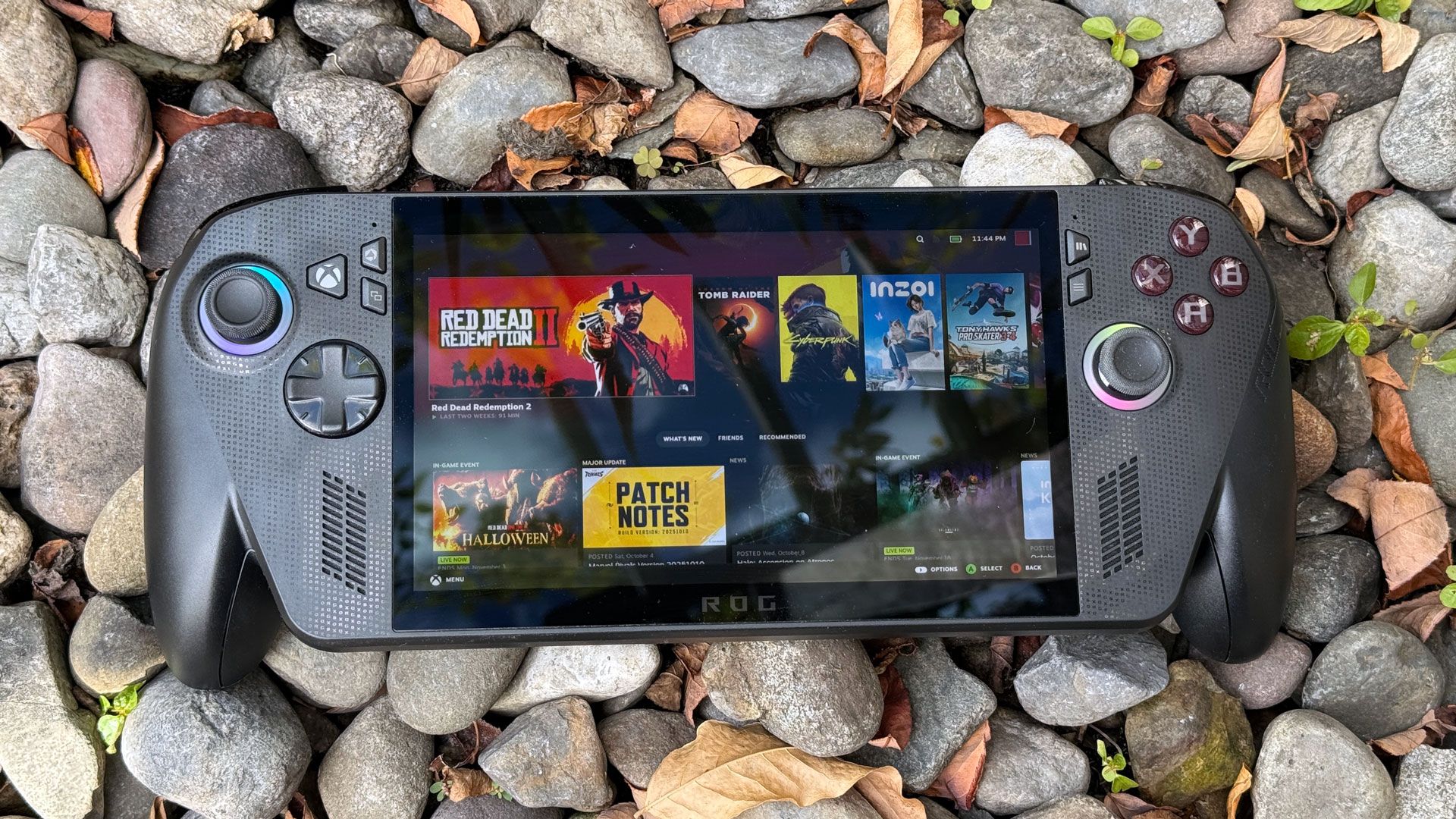
Earlier this year, AMD brought the previously RX 9000-exclusive FSR 4 upscaling tech to Radeon RX 7000-series graphics cards and promised an early 2027 release for RX 6000-series products. Christmas has come early for RDNA 2 and many other Radeon gamers, as Radeon honcho Jack Hyunh has announced an FSR 4.1 release for Radeon RX 6000 series cards, Xbox Series X and Series S consoles, Ryzen Z-series handhelds, and machines with Ryzen AI Max and AI 9 chips today.
To accomplish this feat, AMD says it tweaked FSR 4.1's neural network model to support the INT8 shader hardware (as opposed to the higher-precision FP8 matrix acceleration hardware on Radeon 9000 cards). Additionally, the version specific to handhelds is slimmed down even further, to less than half the size of the full one.
AMD says that compared to FSR 3, games on the aforementioned GPUs and APUs will now deliver better image quality, all else equal. With Cyberpunk 2077 running in FSR Balanced mode at 4K, our quick testing with a Radeon RX 6900 XT shows that running FSR 4 costs just about 13% performance, a small price to pay for sharper and more stable visuals, especially in motion.
And the higher upscaling quality of FSR 4.1 might let gamers use Performance mode where they might previously have used Balanced, or so on, which might offset that performance cost.
There are more goodies in store, too. The Radeon team says that FSR Frame Generation now ought to have better frame pacing, resolving a longstanding complaint with the tech and potentially making for smoother gameplay with framegen enabled. Support for the Vulkan API with FSR 4.1 is set to arrive at some point, as well, a boon for some games and console emulators. Finally, AMD says FSR Ray Regeneration will also be coming to more games, too. The company showed the tech running in Warhammer 40,000: Darktide, and that integration is available now.
To get all this goodness into your GPU, you can download the just-released Radeon 26.10.1 drivers from the AMD Adrenalin application or directly from AMD's website. The updated software also adds support for Call of Duty: Modern Warfare 4, Star Wars: Galactic Racer, and Final Fantasy Resonance. You can check out the full release notes here.
For owners of Xbox and Ryzen Z2-series handhelds, AMD says that an update from their manufacturers will be forthcoming, as those devices depend on OEM-specific drivers.
We're pleased to see that Radeon gamers are getting upgrades for their existing graphics chips along the lines of what Nvidia has been delivering throughout 2025, because the way things are going, it looks like it'll be around 2077 before there will be a new gaming graphics card launch. If you're an RDNA 2 gamer, go give FSR 4 a shot and see what you think.
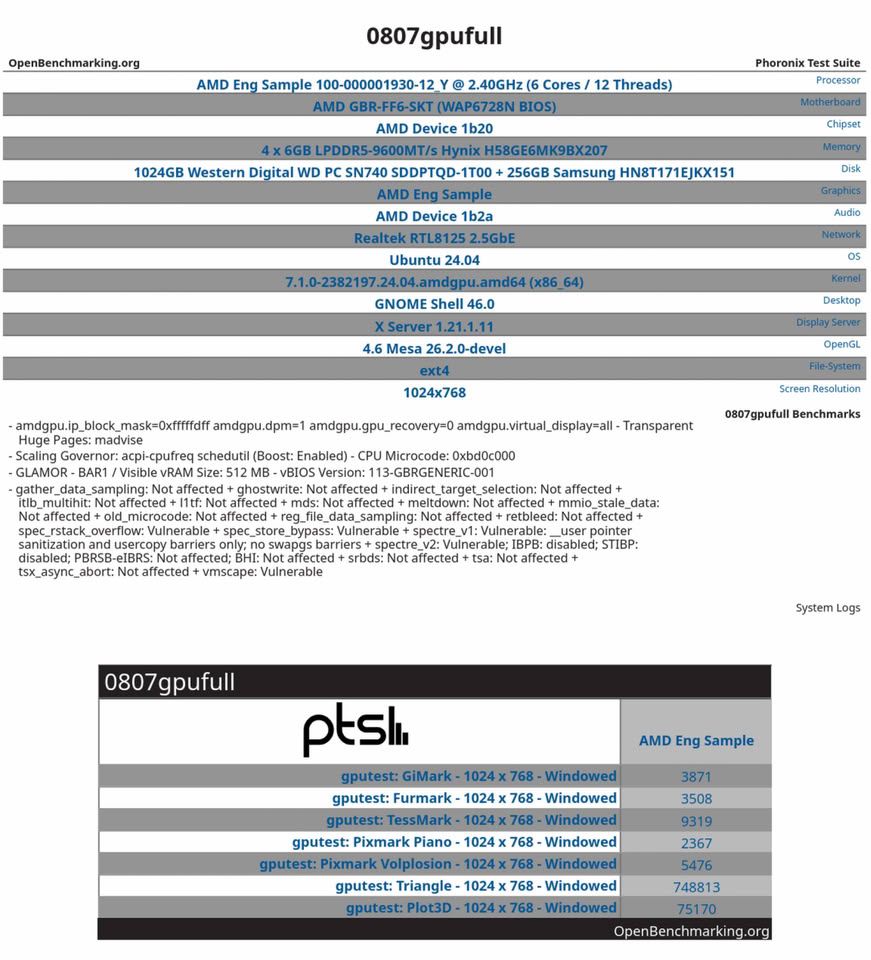
An AMD engineering sample has made an appearance in a listing on OpenBenchmarking. According to a report by TechPowerUp, the chip could potentially be a part of AMD’s upcoming Gainsborough family and a possible candidate for the next-generation Steam Deck handheld console. As per the OpenBenchmarking listing, the chip comes with a six-core, 12-thread processor paired with 24GB of high-speed LPDDR5 memory.
The engineering sample with part number 100-000001930-12_Y was tested on an AMD GBR-FF6-SKT validation board, with the CPU running at clock speeds of 2.4 GHz. The system also features four 6GB SK Hynix memory packages, resulting in 24GB of LPDDR5 memory running at 9,600 MT/s. That’s a big jump when compared to the current Steam Deck, which comes with 16GB of LPDDR5 memory running at 6,400 MT/s, alongside a four-core, eight-thread AMD Zen 2 processor.
(Image credit: OpenBenchmarking)
The benchmark listing also provides some clues about the processor’s underlying architecture. As per Notebookcheck, the sample’s CPU microcode revision corresponds to AMD’s Family 1Ah, model DCh. Linux kernel changes indicate that this model falls within the range reserved for newer Zen 6 processors, suggesting that Gainsborough could use AMD’s next-generation CPU architecture. However, there is no clarity or any confirmation whether it will use standard Zen 6 cores or the denser Zen 6C variant.
The integrated GPU is listed with a clock speed of 2,400 MHz, although its architecture and compute unit count remain unknown. The sample was tested using the GpuTest benchmark suite on Ubuntu 24.04 at 1024 x 768 resolution, resulting in scores of 3,871 in GiMark, 3,508 in FurMark, and 9,319 in TessMark. While the FurMark score is comparable to the original Stam Deck, we can’t really come to any conclusions at this point, as the tests were conducted on an engineering platform using development software rather than a finished handheld. For now, the results do not establish how the chip would perform in games, as power limits, cooling, driver maturity, and the final GPU configuration all contribute to the performance in a compact gaming device.
If these specifications carry over to a future Steam Deck, the additional CPU cores along with the larger and faster memory would provide a meaningful hardware upgrade. That being said, neither AMD nor Valve have confirmed a connection between the Gainsborough family and a future Steam Deck. Thus, it is best to take this with a grain of salt and wait until there is more concrete information in the future.
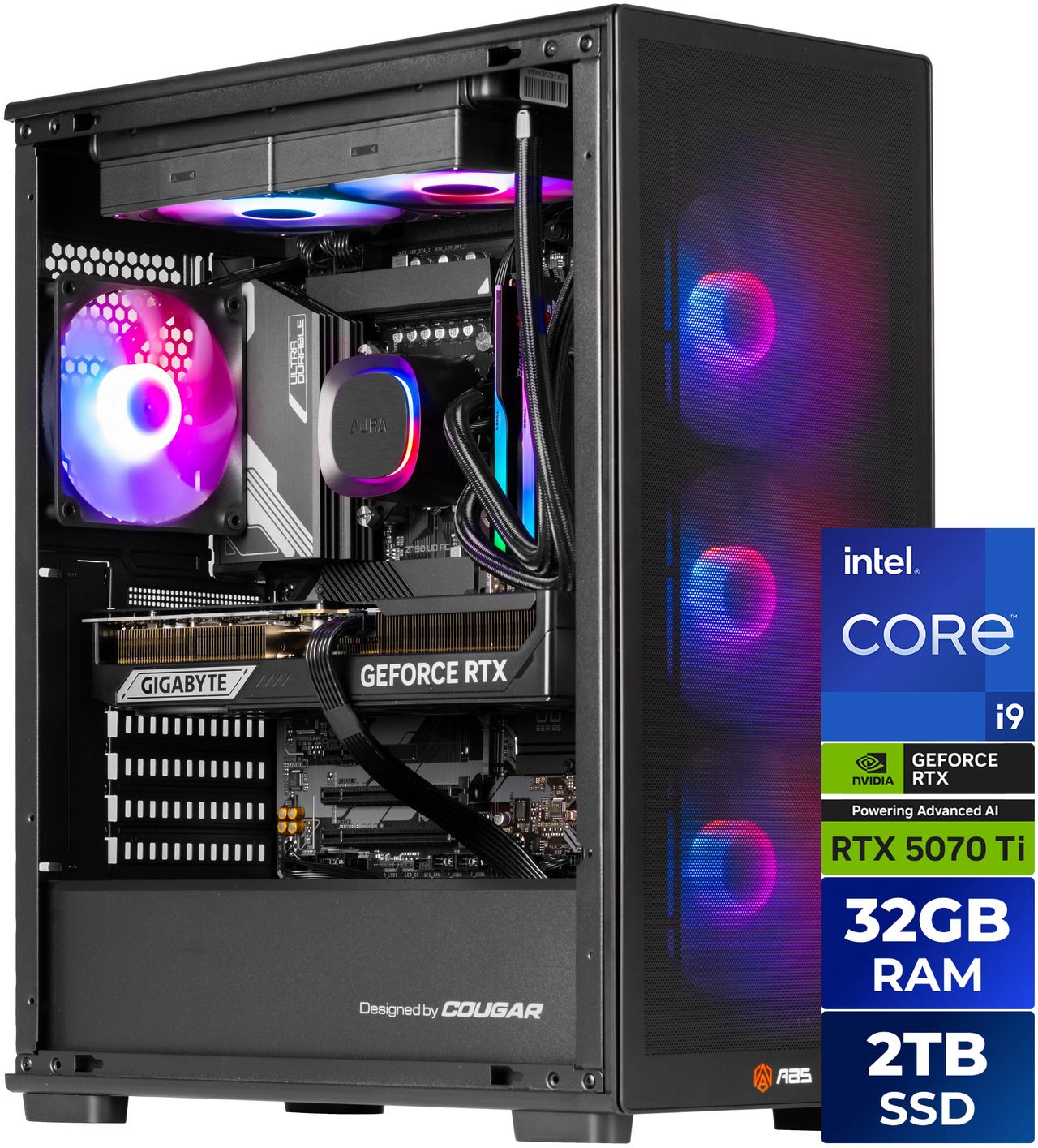
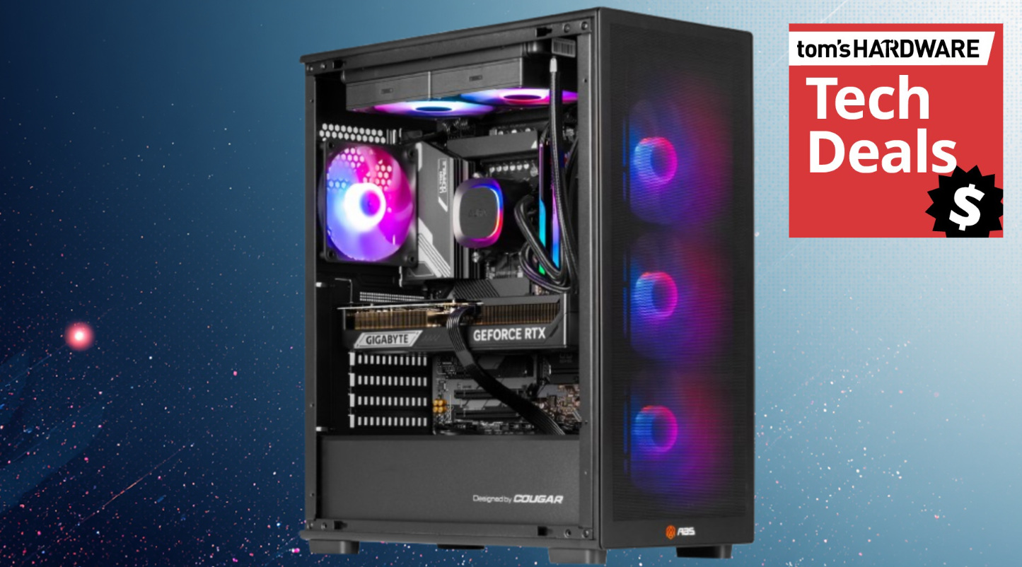
Here we are, nearly a year into the AI pricing apocalypse, and anyone who tried to build a PC during that time relied on some kind of combo deal to bring prices down to something more reasonable. If building a system on your own isn’t in the cards, Newegg is offering a great deal on its own ABS-brand prebuilt, which saves you money, time, effort, and hassle. You can buy the ABS Stratos II Aqua for only $2,549 and start gaming as soon as tomorrow without blowing your budget.
For the money, you get a complete prebuilt gaming system complete focused around the previous generation flagship 14900KF processor, and Nvidia’s capable RTX 5070 Ti 16GB along with a cool looking ABS Stratos II MX220 Black Gaming Case with four pre-installed fans, quality Gamdias Helios ATX/PCIe(3.1/5.1) 850W Gold power supply, 240mm AIO cooler, 32GB of G.Skill Ripjaws M5 RAM, 2TB Team Group M.2 storage, and a Gigabyte motherboard, making this one of the better deals around for a complete gaming system.
The ABS Stratos II Aqua and the mid-tower chassis include an Intel Core i9-14900KF processor featuring 24 total cores (8P+16E) and 32 threads, with speeds up to a smoking-fast 6 GHz. While this isn’t the fastest gaming processor on the market, it still holds its own, especially at higher resolutions, which the video card can handle without issue.
Save big on the Newegg ABS Stratos II Aqua gaming PC. View Deal
The CPU drops into a Gigabyte Z790 US AC motherboard that offers plenty of connectivity, including 10 USB ports on the rear IO (one 20 Gbps Type-C), two M.2 sockets (both PCIe 4.0 x4), and six SATA ports for storage, 2.5 GbE and integrated Wi-Fi, and will handle the flagship-class i9-14900KF processor. It also pairs well with 32GB of G.Skill Ripjaws M5 Neo RGB DDR5-6000 RAM and a 2TB Team Group NV5000 PCIe 4.0 x4 SSD. ABS also includes the Gamdias Aura GL240 V2 240mm RGB AIO to help keep the unlocked, high-performance processor running smoothly.
FutureFutureFutureFuture
The GPU is Gigabyte’s Windforce RTX 5070 Ti SFF OC, with three fans (2.5-slot-wide) and an all-black look that should pair well with the motherboard and other components. The RTX 5070Ti is a capable graphics card for high-refresh-rate 1080p gaming, 1440p gaming, and even some 4K titles. You won’t find any RGB lighting on this card, but the triple-fan cooling solution will keep the card running cool and quiet.
FutureFutureFuture
While it can be cheaper to gather the parts and build your own, it isn’t for everyone. If you build your own and it breaks, troubleshooting is on you. Some people just want to open a box and start gaming and not have to worry about support. ABS backs its systems with a 1-year warranty, so if anything goes wrong, you can easily get it fixed.
For $2,549 (a $450 savings), you can buy a complete, warrantied gaming system that will run anything you throw at it with aplomb without completely emptying your bank account.
Chinese technology giants ByteDance, Alibaba and Tencent have reportedly spent over $35 billion on orders for more than 3 million Nvidia RTX Pro 5500 workstation GPUs. The huge order for the RTX Pro 5500, fully compliant with U.S. restrictions on exports of AI-capable GPUs to China, is reportedly far beyond Nvidia's planned production for this card. As a result, Nvidia has, according to sources who spoke to Reuters, told its customers that it isn't in a position to fill the orders as it far outstrips its planned production for this GPU.
The RTX Pro 5500 is a workstation GPU with the same number of CUDA cores as its flagship RTX 5090 GPU, but with 84GB of GDDR7 memory attached, making it a good option for AI applications. The RTX Pro 5500 is a popular choice at the moment for Chinese buyers as exporting it isn't currently restricted by the U.S. government. It's less powerful than the H200 and B300, Nvidia's AI-focused GPUs for the enterprise market, but those GPUs remain either banned or heavily restricted. As China competes with the U.S. in the race to produce newer, better AI models, GPUs like the RTX Pro 5500 continue to be indispensable.
The report reveals some interesting data about the Chinese tech firms orders. Two of its sources revealed that the cards are priced at around $11,400 each, reaching a total order value of $35 billion. Meanwhile, another source suggested that Nvidia has informed its partners that it may only be able to deliver enough cards to meet between 5% and 10% of the demand. Meanwhile, Nvidia is reportedly in a position to only produce 3 million RTX Pro 5500 cards globally in 2027.
Neither Nvidia nor the three Chinese companies have confirmed any of this on the record. However, an Nvidia spokesman told Reuters that demand from the Chinese market for these chips has faced "unprecedented growth since 2022" since export restrictions were introduced. "U.S. firms continue to be restricted by a combination of outdated U.S. export controls, which cover gaming products released nearly half a decade ago, and China's own limits on U.S. imports."
While trade hostility between the U.S. and China shows no sign of abating, demand for Nvidia's GPUs hasn't slowed down, despite U.S. attempts to restrict Nvidia's ability to export to China. Meanwhile, export-restricted Nvidia AI chips continue to reach China despite the restrictions, bypassing the Trump administration's efforts in the process.
Popular graphics post-processing injector software ReShade, commonly used to mod DLSS 5 into unsupported games, now has a foveated imaging add-on, including another standalone project that doesn't need precursor software, allowing DLSS 5 to affect only what's in view, reducing GPU load and increasing FPS.
Foveated imaging is nothing new; it's a technique that's been used in VR to increase performance. It works by only rendering what's in view, often increasing the resolution in the center and reducing it at the edges. Our eyes work in a similar way, with the clearest image in a small area in the center of your vision, blurring on the edges. With foveated rendering, you barely notice the lower-resolution edges as the peripheral vision is less concerned with fine details.
Instead of varying the resolution of the image, however, it varies the level of detail in DLSS 5 Neural Rendering. DLSS NR loads a whole AI model into your GPU and renders images in real time, making it a resource-intensive task; but the task is minimized greatly when most of the detail is only asked for in the middle of the image. That's what projects like maximedgoulet’s Foveated DLSS5 and ClarkCheekyKent’s CheekyFoveatedDLSS aim to do; with Foveated DLSS being a ReShade add-on and CheekyFoveatedDLSS capable of being a standalone integration.
Both implementations allow you to adjust the size of the center area with the highest rendering quality, with independent width and height adjustments to suit your personal situation, as some people have a larger focus area than others or have a different monitor distance. You can also adjust the render fall-off rate, so the image quality lessens more quickly or slowly past the focus area.
As Maximedgoulet's implementation is an add-on for an injector, the pipeline is quite long compared to the standalone integration of CheekyFoveatedDLSS, which Reddit comments claim is more convenient and more polished. Though both show a big improvement in performance, Maximed's Reddit post on Foveated DLSS5 claims an improvement from 48 to 80FPS in The Witcher 3 with 2x Multipass at ultrawide 7680x2160p on an RTX 4090. Considering Maximedgoulet’s 4090 could not handle DLSS-NR on an ultrawide, this implementation might genuinely be feasible to make Neural Rendering more playable.
Nvidia has earned billions selling AI accelerators, but with the emergence of agentic AI, CPUs are going to play a considerably more significant role than before, which creates new opportunities for the company. Reutersreports that Nvidia has secured a major design win with its Vera CPUs with AI cloud provider Modal. According to Modal, preliminary evaluations showed that Vera could deliver twice the throughput of its existing AMD and Intel processors, although the company does not intend to cease using CPUs from its current suppliers.
Modal provides cloud infrastructure that enables AI developers to deploy AI agents that can perform complex operations autonomously over extended periods. Such workloads require substantial CPU resources for software execution, data processing, and other tasks that cannot be efficiently handled by GPUs. Modal currently relies exclusively on AMD and Intel processors for these operations, but its tests indicate that Nvidia's new Vera CPUs could significantly improve performance in its specific workloads. Of course, since Vera is based on an Arm instruction set architecture, Modal's decision to adopt Vera will require substantial modifications to its software. Nevertheless, Modal believes that the potential performance improvements justify the additional engineering effort.
The reported 2x throughput advantage is particularly interesting because agentic AI workloads can involve numerous independent tasks that compete for CPU cores, cache capacity, and memory bandwidth. However, Modal has not disclosed detailed benchmark configurations it used, specific AMD and Intel processor models, or performance-per-watt figures. Consequently, it remains unclear whether Vera's advantage is enabled by advantages of its Arm v9.2-based Olympus CPU cores that can decode and execute up to 10 instructions per cycle, its memory subsystem with 1.2 TB/s of bandwidth, or other architectural characteristics. Also note that tests compared Vera against currently available AMD and Intel processors rather than their upcoming generations that will compete against Vera in the coming years.
Since Modal cannot port all of its software to Arm ISA overnight, the company will continue using x86 CPUs from AMD and Intel, according to Modal chief executive Erik Bernhardsson. Rather than sticking to one ISA for everything, Modal intends to operate a heterogeneous server fleet and select the most suitable processors for each workload. Naturally, the company intends to evaluate upcoming AMD and Intel processors once they become available to make its choices in the future.
For Nvidia, the agreement represents a major step toward making Vera a standalone server processor that commands a major share of the server market. The company expects Vera sales to generate at least $20 billion during its current fiscal year and estimates the potential total available market for these CPUs is approximately $200 billion. The company is on track to sell at least four million Vera CPUs in fiscal 2026.
The announcement comes shortly after Modal secured $750 million in financing led by Accel, which valued the company at $15.75 billion. Modal expects its annual revenue to reach $1 billion within the next year. The company's service consumption has increased 3X in the last 12 months, while revenue has surged more than 15 times compared with the previous year, Reuters reports.
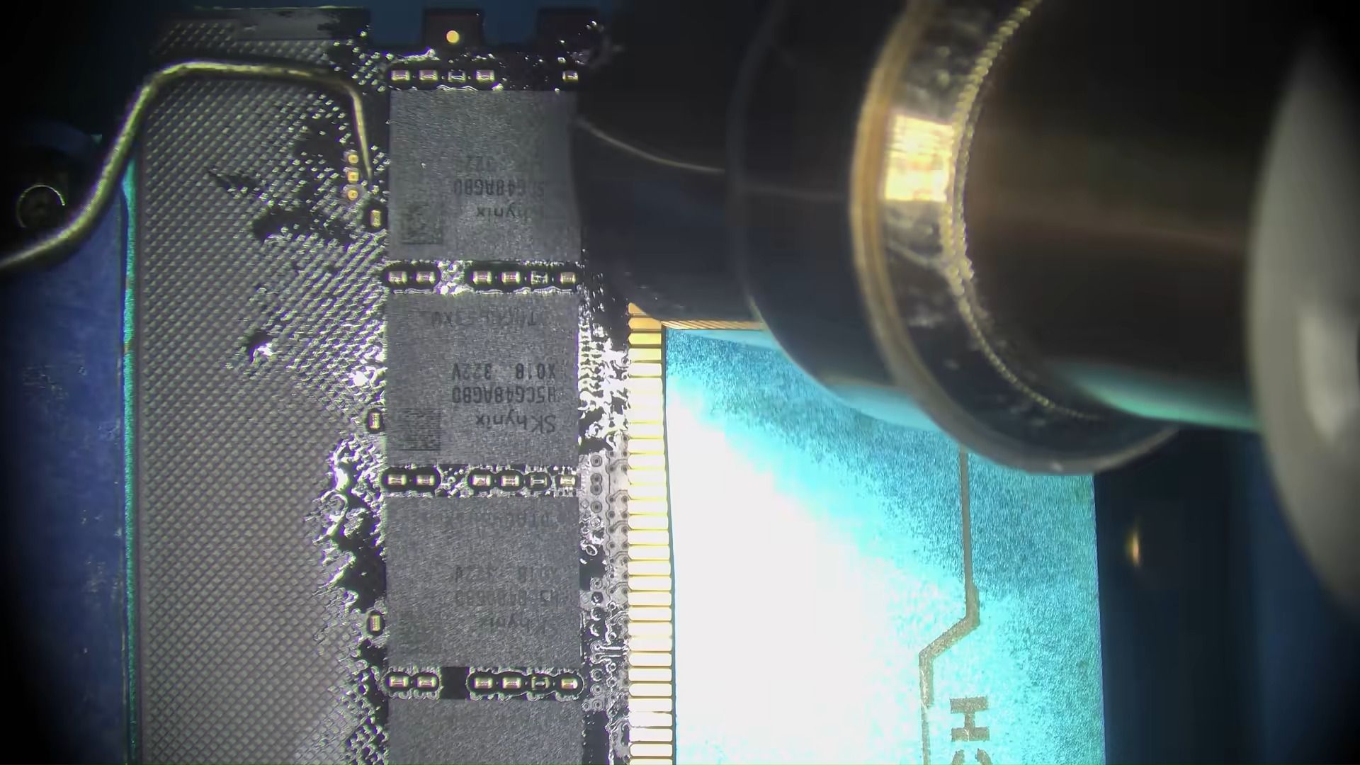
What if you could buy a cheap used DDR5 SODIMM (laptop memory) kit and transform it into a super-fast DDR5 desktop kit? That’s what electronics hobbyist Blighted Agent recently did when they succeeded in converting a SK hynix 2x 16GB DDR5-5600 SODIMM kit they got from Facebook Marketplace for $120 into a 2x 16GB DDR5-7800 desktop kit, claimed to be worth around $1,000. They also had to buy some blank DDR5 desktop memory PCBs from AliExpress for around $16 each, and a set of heatsinks for around $18.
In the above video, our hero says they bought the donor laptop 2x 16GB DDR5-5600 sticks for just $120, which is a bargain. With extra bits and pieces from AliExpress (desktop DDR5 PCBs, etc.), the total bill of materials came to $175. Blighted Agent comments that the SODIMMs used what he believed to be SK hynix A-die modules, which are the same as the ICs used in expensive desktop DDR5 modules like the G.Skill Trident Royal line.
The process began with taking the memory ICs from the donor modules using a hot air station. Then they were cleaned and had 0.45mm leaded solder balls added, using a DDR5 stencil, reballing jig, and hot air. Next, the blank desktop DDR5 PCBs were prepared. A little solder was added to the plethora of BGA connectors to be ready for the memory chips to connect to.
The old DDR5 ICs and the new desktop modules could now be mated, using flux, the preheater, hot air, and watching and prodding carefully with a dental pick. Blighted Agent’s experience lets him know when the BGA chips have successfully mated with the PCB. You can eyeball when they pop precisely into place due to surface tension, and offer up a modicum of resistance to pick prodding.
Finally, the enthusiast added the SPD chip and BIOS chip from the SODIMMs to the new desktop DIMMs. These new desktop DIMMs were quickly tested in a PC before they were finished off with carefully applied thermal pads and the fancy-looking heatsinks.
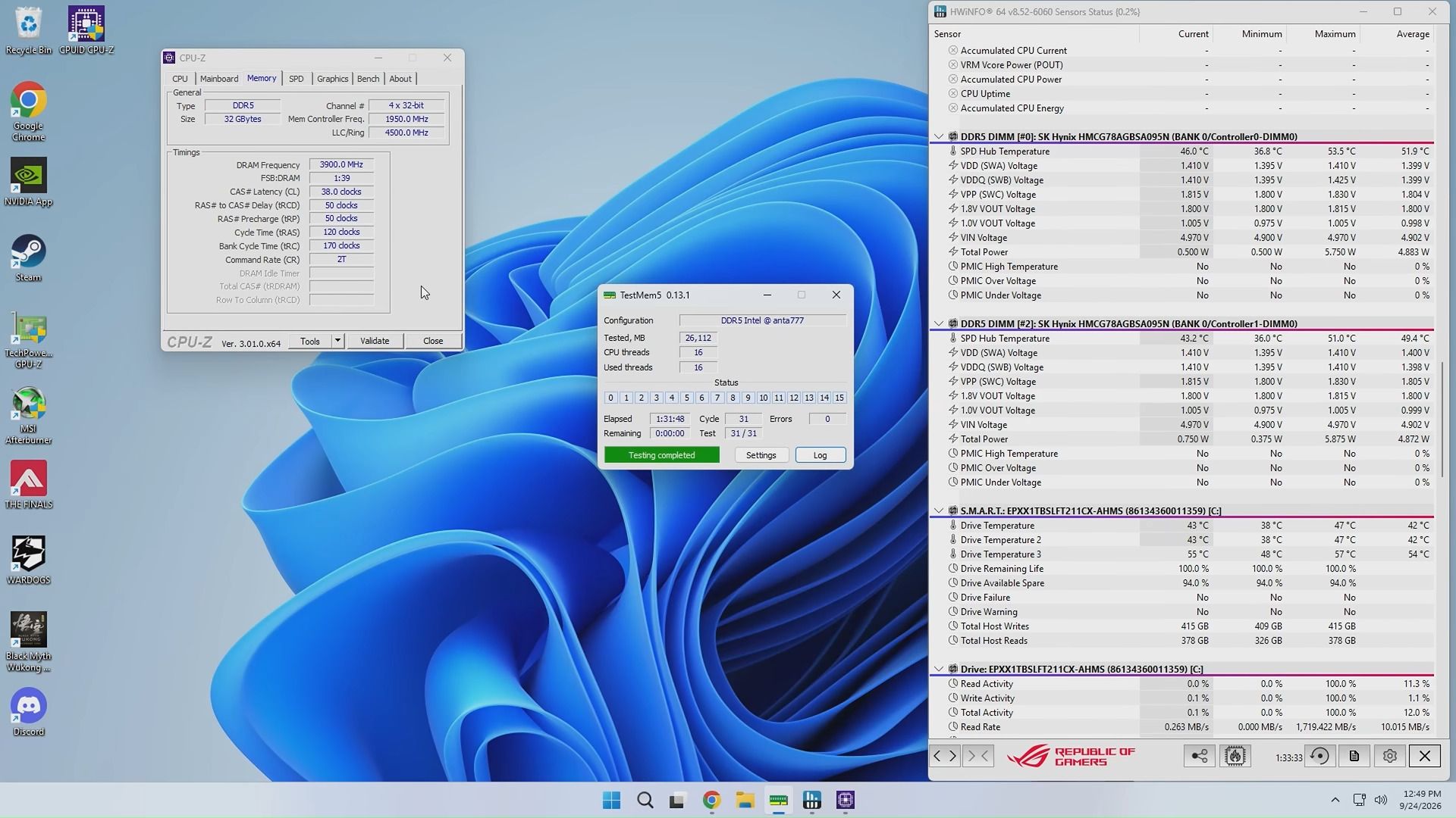
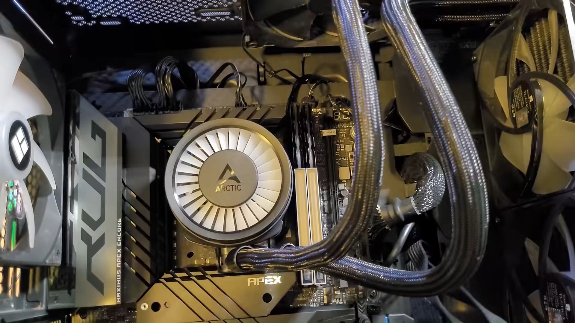
Blighted Agent felt lucky that there were no issues with the newly created desktop modules. There’s a lot of intricate things that can go wrong during such a process. The initial boot verification showed them recognized in his Asus ROG Maximus Z790 Apex Encore motherboard as two “SK hynix 16,384MB 5600MHz” modules, which was correct. Some tuning resulted in rock-steady performance at DDR5-7800 CL38 and 1.40V. This was verified by stress testing for 90 minutes, which the enthusiast reckons was ample for a gaming PC. It is very likely a better result than using those mechanical SODIMM-to-DIMM converters you can buy, which can be problematic.
Blighted Agent seems to specialize in BGA soldering work, and has also successfully upgraded several graphics cards with double the VRAM. Though videos like this are edited to be brief, and they make the process look easy, the TechTuber admits there is a lot that can go wrong during this kind of rework. Moreover, with RAM modules, they lack the testing equipment to locate an issue with any particular IC on the PCB. So, if this module didn’t work, they might have ended up in a world of pain, not knowing which memory chip had an issue due to either an internal fault or a BGA soldering glitch.
Blighted Agent on YouTubeBlighted Agent on YouTubeBlighted Agent on YouTube
Looking around at used DDR5 SODIMMs, it looks like Blighted Agent was very lucky to get a used working 32GB kit for $120. I just checked eBay U.S., and the best deal there was $320. Meanwhile, the best price for a new 32GB DDR5-6000 kit seems to be $449 at the time of writing.
We reported on Russian enthusiast VIK-on succeeding in a similar project earlier this year, but all their costing was in Rubles, and they went the extra mile in flashing custom firmware so the remade modules would be auto-detected with 6400 MT/s XMP support on most motherboards. In late 2026, DDR5 RAM continues to be too expensive.
Panchovix on GitHub recently released a VBIOS configurator for RTX 30-to 50-series cards that doesn’t require flashing. The loader provides a UI for easy configuration and lowers the risk of bricking your GPU by avoiding a risky flash process, and it's available for Linux, too.
Software like MSI Afterburner or ASUS GPU Tweak is often the go-to tool for quickly changing your graphics card’s settings; however, those tools have hard limits to how much you can push the graphics card. If you want to tweak your GPU beyond the firmware’s set limits, you can change it by tweaking the parameters in the VBIOS. Configuring VBIOS is similar to changing BIOS settings in the BOOT menu. With the VBIOS loader, you can change settings beyond the firmware’s hard limits.
The way it works is by storing the modified VBIOS image in the GPU’s register key; as the Nvidia driver looks for a VBIOS override on startup, it finds the VBIOS image and restarts, applying the override settings. The flash chip on the graphics card is not overwritten, reducing the risk of bricking your GPU. However, this does not protect the card from any extreme settings that could destroy electrical components; it merely provides a safer and more convenient way to adjust and apply VBIOS settings, including a way to roll back to the default VBIOS settings should you face any instability.
Bricking a flash chip isn’t as catastrophic as it seems, however. As long as you have a backed-up version of the VBIOS, you can easily buy an SPI flash chip programmer or even build your own using a cheap Raspberry Pi Pico and its many clones; sometimes programming the flash chip may not even require desoldering. Programming a flash chip is very tedious and inconvenient, though, which is why avoiding the risk of a botched flash process altogether is so appealing.
Unless you’re familiar with power delivery, voltage tables, and the patience required to test for hours, we wouldn’t recommend jumping into this unless you’re prepared to risk your GPU. However, you can still safely take advantage of this software by tweaking the fan curves and other settings you’ve applied and tested in software like MSI Afterburner if, for some reason, the startup settings don’t stick. This software will give your GPU new default settings that override at every startup, so long as Nvidia doesn’t remove the registry key that allows the VBIOS override.
Arm announced last week that its AGI CPU, the company's data center CPU for agentic AI workloads, delivers twice the performance per rack as AMD EPYC 9755, calculated from chip performance and server-power assumptions measured across seven workloads. The claim stems from modeled rack results from tests aligned with Arm’s new CPU evaluation methodology, developed with support from Fujitsu, Meta, and OpenAI.
The results — verified in an Arm-commissioned independent analysis by Signal65 — do not establish the AGI CPU as the overall leader for agentic AI, as they apply to the selected processors, workloads, and configuration. They also use the specific Arm-developed evaluation methodology that Arm says should be the new standard for assessing performance. However, other chipmakers like AMD and Intel make performance claims based on different benchmarks. So, how is Agentic AI evolving CPU performance benchmarks, what does Arm propose to measure, and how do the different approaches compare?
Arm’s new CPU evaluation methodology
Agentic AI is changing the role of CPUs in modern AI data centers, requiring them to handle complex, multi-step workflows. Beyond inference, which the accelerator handles, AI agents execute tools, retrieve data, and maintain state within isolated environments, acting like virtual users. The CPU handles these critical surrounding workloads, from running those tools and serving database or API requests to preparing data and coordinating work for accelerators.
As these workloads scale rapidly with agentic capabilities, it becomes increasingly important to gauge CPU performance not just by how many agents can run concurrently, but also by how much useful work gets done. Arm argues that CPU performance is increasingly defined by how much useful work a system can sustain while staying responsive. Supporting more agents simultaneously offers limited benefit if their executions throttle or accelerators have to sit idle waiting for the CPU. Power, cooling, and physical space also limit how much hardware operators can deploy, extending the performance question to the rack.
Arm’s proposed methodology for evaluating CPU performance, developed with support from Fujitsu, Meta, and OpenAI, centers on representative agent workloads, repeatable CPU measurements, and validation against end-to-end task outcomes. In practical terms, the methodology identifies the tools and services an agent uses, measures their CPU performance under controlled conditions, and checks whether improvements help the agent complete its task. For example, a database test can establish how quickly a system handles transactions. An end-to-end evaluation would then examine whether faster database access actually improves the workflow that depends on it.
Executing the second aspect of the methodology, making these comparisons repeatable, presents another challenge, as an agent might choose different commands or take a different route through a task each time it runs. Model inference and remote services also introduce delays. Arm proposes replaying recorded agent actions to separate CPU performance from this variability, allowing different systems to execute a consistent sequence of work. Its whitepaper sets out a framework for selecting and interpreting these measurements, leaving the industry to develop an agreed benchmark suite and scoring approach.
To evaluate the CPU work described in its framework, Arm ran seven workloads — spanning tooling, agentic workflows, and reasoning/planning, plus Sandbench, which measures sandbox-creation overhead for agent execution — on its AGI CPU and AMD’s EPYC 9755. The tests combine established server applications with benchmarks focused on agent workflows.
Workloads and breakdowns
Workload
What it represents
Metric
MySQL
Transactional database behind agent tools
Transactions per second
NGINX
Web and API request handling
Requests per second
Milvus
Vector search for retrieval
Queries per second
Terminal-Bench 2
72 agent task types in sandboxed containers, 128 copies at once
Task completion time
SWE-bench replay
Software-engineering agent workflow, 259 tasks
Tasks per minute
fastText
CPU word-representation training
Words per second
vLLM CPU overhead
CPU serving overhead with model compute bypassed
Requests per second
The vLLM result measures the CPU work around model execution, not GPU inference throughput. Similarly, the report’s “reasoning/planning” category groups supporting CPU workloads and does not assess how intelligently a model reasons.
ARM AGI CPU vs AMD EPYC 9755
For the tests, Arm used two AGI CPU configurations because of hardware availability: a 128-core chip at 2.8 GHz with DDR5-7200 for Terminal-Bench 2 and SWE-bench replay, and a 136-core chip at 3.2 GHz with DDR5-8000 for the other five workloads. The AMD comparison used one socket of the 128-core EPYC 9755 with DDR5-6400. Both platforms ran the same benchmark scripts but used different software environments. Arm used custom Linux 7.1.3 builds, with Ubuntu 24.04 for most tests and Ubuntu 26.04 for SWE-bench, while AMD’s main recorded configuration used Ubuntu 24.04 and Linux 6.8, with settings varying by test.
At the chip level, Arm’s AGI CPU won the majority of comparisons when compared to its AMD counterpart in five of the seven tests. With the EPYC 9755 as the baseline, Arm led by 9% on Terminal-Bench, 13% on SWE-bench, and 97% on fastText, but lagged by 12% and 5% in MySQL and Milvus throughput, respectively. On average, the AGI CPU led by 20% (1.20x) per-chip advantage, calculated across the seven normalized performance ratios.
Results
Workload
Measured per-chip performance vs EPYC 9755
Modeled per-rack performance vs EPYC 9755
MySQL
0.88x
1.43x
NGINX
1.20x
1.95x
Terminal-Bench 2
1.09x
1.93x
SWE-bench replay
1.13x
2.00x
Milvus
0.95x
1.54x
vLLM CPU overhead
1.16x
1.88x
fastText
1.97x
3.19x
Arithmetic average
1.20x
1.99x
At the rack level, Arm’s modeled performance averages 1.99x AMD’s, with a lead in all seven workloads. The model uses rated server-power estimates of 950 W for the 128-core Arm configuration, 1,050 W for the 136-core version, and 1,700 W for AMD, including memory and other system components. After reserving about 8% of a 24 kW rack budget for networking and power distribution, this leaves room for 23 or 21 Arm servers versus 13 AMD servers.
For SWE-bench, the 2.00x per rack result was obtained by multiplying the roughly 1.13x chip result by 23/13. The larger gain comes from fitting more servers into the same power budget. Furthermore, these projections use modeled whole-server power, not throughput measurements from two fully populated racks.
Arm’s model also gives the AMD servers about twice as much RAM: roughly 2 TB against 1 TB for Arm. It allocates 4 GB per hardware thread, with each AMD core supporting two threads while each Arm core supports one. This puts the memory-power allowance at 336 W for AMD and 192 W for Arm. Signal65 also calculated what happens when memory is allocated per physical core. In this setup, AMD’s memory and power allowance falls, and Arm’s average modeled rack advantage drops from 1.99x to approximately 1.81x. The usefulness of the 2 TB AMD configuration depends on how much memory the workloads actually need, as SMT does not inherently require twice the memory.
To verify the findings, Signal65 remotely observed Arm’s test runs and examined the original logs, result files, scripts, and configuration records. A separate review team rebuilt the calculations with its own code and reproduced all seven results within 0.5%. However, Signal65 did not run a separate hardware rerun in its own lab. In addition, Signal65 could independently confirm BIOS and memory settings for only the EPYC 9965 system. These settings were unavailable for independent verification on the Arm and EPYC 9755 systems. Along with the software differences, these gaps slightly affect the certainty with which the results can be attributed to the processors themselves.
Arm’s approach vs AMD and Nvidia
While Arm believes its methodology should be the standard, it does not hold a monopoly on how the industry evaluates agentic CPU performance. For example, AMD promotes agents per watt, dollar, and rack. Footnotes on its EPYC 9006 page identify available CPU threads as a proxy for agent capacity, with actual throughput depending on the workload and system. Its separate workload analysis models a 100 kW rack and claims 2.37× performance for EPYC 9965 over Nvidia's Vera, using a geometric mean across six infrastructure workloads.
Nvidia, on the other hand, emphasizes Vera’s single-thread performance and memory bandwidth, and says a 256-CPU rack supports more than 22,500 concurrent CPU environments. These numbers describe different things and do not directly imply any specific advantage. Methodologies vary across manufacturers by workload, power assumptions, and aggregation methods, making direct CPU comparisons complex. The current comparison is against AMD's fifth-generation “Turin” processor with 128 cores. The company launched its latest sixth-generation EPYC 9006 “Venice” family this year, dedicated to agentic AI.
The DLSS-NR project on AMD by Daniel Blanco was first released on September 3, 2026, bringing DLSS 5 Neural Rendering to Radeon GPUs; in the latest 0.8.0 update, however, it makes all the main DLSS features available, featuring DLSS SR, Frame Generation, Ray Regeneration, and the newest DLSS NR model, along with more performance improvements.
While AMD has equivalents for most DLSS features like FSR upscaling, frame generation, ray regeneration, and anti-lag, it’s not as commonly supported by most games compared to Nvidia’s offerings. Even if players could use the AMD equivalent features, Neural Rendering is one that AMD just doesn’t have an equivalent for yet, which is why mods like DLSS-NR on AMD were made.
Daniel Blanco wanted to fill the gap with NR in its initial release, but in the latest update, he added all the DLSS features: DLSS Ray Reconstruction, Super Resolution 4.5, Frame Generation, and the latest 310.9.16 improved Neural Rendering build that we covered recently with modders using it on unsupported games. Interestingly, the update notes say it includes FSR 4.1.1 upscaling; AMD GPUs already use FSR, but having FSR 4.1.1 specifically gives the mod a consistent version of FSR to work with, instead of having to be compatible with the various implementations of FSR in different scenarios.
The mod currently supports three generations of Radeon GPUs: RX 9000, 7000, and 6000 (RDNA4, 3, and 2, respectively), in any DirectX 12 game that uses FSR, DLSS, or XeSS. You can install the mod by downloading the NeuralHub mod loader, which provides a UI for you to install it into the games it detects. You then enable FSR, DLSS, or XeSS in the game, and the mod will insert itself into that upscaler pipeline, allowing it to inject any of the settings you configured for the game in the NeuralHub; it even provides an overlay to tweak the DLSS settings without leaving the game.
With a few improvements from the first version, the developer says the output quality is very similar to what DLSS produces on Nvidia GPUs natively, except for “some effects that may not be working 100%.” In the developer’s own testing, he found it to be playable at 90-100FPS at 1080p on an RX 9070 XT, while saying that he’s making improvements every day, planning to match the performance of a 5070Ti.
Real-world results are mixed, however, as Reddit users report showing no performance loss over native FSR, while others experience losing single-digit FPS to up to 25% lower FPS in various games. The developer still has to account for many factors since there are a myriad of PC configurations, but the results look promising as he bridges the gap between AMD and Nvidia GPU features — though it won’t work with anti-cheat, unfortunately.

 Login