❌

Reading view

Intel installs production tools at Fab 62 in Arizona, provides updates on Ohio chip fab

Intel on Wednesday announced that it had started installing production tools at its Fab 62 in Arizona, and the fab is on track for mass production by late 2028. The company also reported progress on its Ohio One manufacturing complex and confirmed that it has integrated High-NA EUV lithography into high-volume manufacturing (HVM). Meanwhile, Intel continues to invest in its leading-edge process technology R&D, advanced packaging, and photomask production capabilities in the U.S., which puts the company ahead of the competition.

"There is an important difference between technologies made in America and technologies that are truly American-made," wrote Naga Chandrasekaran, executive vice president and chief technology and operations officer, Intel Foundry. "The difference lies in the research and development process that transforms ideas into manufacturable technologies."

Fab 62 to begin operations in 2028

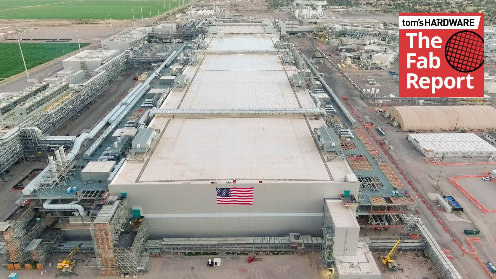
Intel completed construction of its Fab 62 shell some time ago; now it is time for the company to begin installing production tools, which is what it is doing now. Intel expects the new facility to become operational before the end of 2028, although it has not disclosed when it intends to begin high-volume production or which nodes it will produce.
Intel

(Image credit: Intel)

Intel has not officially assigned Intel 14A to Fab 62, although the facility has been discussed as a potential manufacturing site for the node. Meanwhile, there is an important distinction between Intel's original plans for Fab 62 and its current commitments. When Intel announced Fab 52 and Fab 62 in Arizona, it said the two facilities would manufacture its most advanced process technologies, including Intel 20A (2nm-class) and 18A (1.8nm-class). Intel subsequently designated Fab 52 for Intel 18A manufacturing. Yet, Fab 62 remains unassigned.

Given Intel's manufacturing process roadmap disclosed earlier this year, Fab 62 will be able to make chips on 18A, 18A-P, and 14A nodes. Intel currently manufactures Intel 18A chips at the neighboring Fab 52, whereas Fab 62 could potentially accommodate either additional Intel 18A capacity or the company’s next-generation Intel 14A process technology. However, Intel has yet to confirm its plans for the facility.

The facility will become Intel's Fab 62, the sixth high-volume semiconductor manufacturing fab at its Ocotillo campus, which has served as one of the company’s primary production sites for decades.

Intel has also not revealed Fab 62's planned wafer processing capacity, or the amount of capital expenditures required to complete the facility. Nevertheless, the installation of production equipment indicates that the project has progressed beyond construction of the building itself. The new fab will expand Intel’s manufacturing footprint in Arizona, where the company already produces leading-edge processors and operates advanced packaging, assembly, and testing facilities.

Intel confirms High-NA EUV insertion into mass production

Another noteworthy disclosure concerns Intel's deployment of High-NA EUV lithography. Intel was the first chipmaker to install a commercial High-NA EUV scanner at its D1X fab near Hillsboro, Oregon, and subsequently integrated the tool into high-volume manufacturing to produce its Panther Lake and other chips.

The Gordon Moore Park at Ronler Acres in Oregon is where Intel develops its most advanced logic process technologies and initiates volume production of the latest processors. Usage of High-NA EUV to produce select tiles for Panther Lake CPUs at D1X is a natural fit for the development fab, as it helps Intel to better understand how these lithography systems work. Meanwhile, it seems (though Intel has not explicitly confirmed) that, for now, High-NA EUV scanners are used to produce the same circuits as Low-NA EUV machines, so the use of next-generation lithography systems does not necessarily provide significant advantages over existing litho scanners.

Ohio One reaches another construction milestone

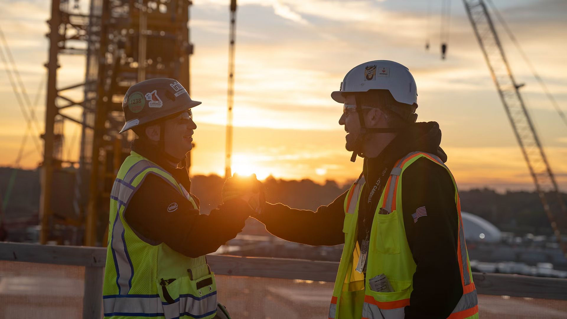
Intel has also made progress with its 'Ohio One' manufacturing complex in New Albany, Ohio. Construction workers recently installed the first major structural truss at the site's first semiconductor fab, which represents a milestone in the development of the company's manufacturing operations in the state. The project is clearly an important part of Intel's long-term strategy to expand domestic production of chips using leading-edge process technologies for years to come.
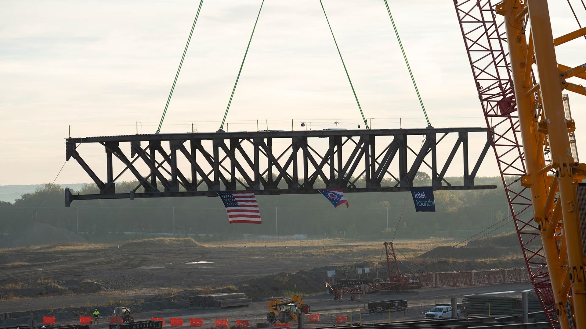
Intel

(Image credit: Intel)

Unfortunately, Intel did not provide an updated construction schedule for Ohio One or disclose when the first fab is expected to begin operations. Intel also did not reveal which process technology the facility will eventually use or the estimated manufacturing capacity it will provide. Therefore, while construction continues, which is good news, the announcement does not clarify exactly when Ohio One will contribute to Intel's output.

Other investments across the U.S.

In addition to leading-edge manufacturing capacity in the U.S., Intel continues to invest in advanced packaging technologies. Oregon serves as the company's main research and development center for advanced logic and 3D interconnect technologies, while Arizona hosts advanced packaging R&D, assembly, and testing operations. Intel uses its site in New Mexico to produce its complex multi-chiplet processors relying on advanced packaging methods — starting with modest EMIB and all the way to next-generation EMIB-T and Foveros technologies.

Mask

(Image credit: Intel)

Also, Intel recently broke ground on a new photomask manufacturing facility in Santa Clara, California. The new facility will be an important part of Intel's supply chain in the U.S., as the company will be the only chipmaker in America to develop and produce chips using leading-edge nodes completely in the U.S. (both Samsung and TSMC currently lack leading-edge process R&D in America; they do not run their own photomask shops in the U.S., and Samsung has abandoned its plan to build an advanced packaging facility in Texas). Of course, Intel critically depends on tools from Europe and materials from Japan, but even as its major rivals invest hundreds of billions in their U.S. production capacity, Intel remains ahead.

To highlight its American supply chain, Intel disclosed that its U.S. operations involve more than 4,500 suppliers across 49 states, as its annual domestic expenditures exceed $29 billion. The company stressed that domestic semiconductor leadership requires not only wafer fabrication capacity but also research, process development, advanced packaging, and a comprehensive supply chain.
  •  

Southeast Asia Hits 243 Million AI Users: Google's Report Reveals a Major Challenge

Southeast Asia has 243 million generative AI users, but paid adoption remains low. Businesses now face the challenge of turning widespread usage into revenue through enterprise tools, AI-powered commerce, and infrastructure investment.
  •  

ASML and other critical semiconductor equipment suppliers expedite shipments to Musk's Terafab

Elon Musk says ASML and other critical semiconductor equipment suppliers have expedited shipments for the ambitious Terafab semiconductor manufacturing facility, supporting his aggressive timeline for the joint megaproject between Tesla and SpaceX. He made the announcement during a live broadcast of SpaceX's Q3 2026 earnings call on X yesterday, October 20. Musk also said the company is targeting volume chip production at the project's primary facility in Gibbons Creek, Texas, by the third or fourth quarter of 2028, emphasizing that the timeline is highly aspirational and carries "big error bars."

"These are very aggressive dates, and we're very appreciative of ASML and all of our other suppliers in accelerating equipment deliveries in order to achieve this outcome," said Musk, CEO of both companies behind Terafab. SpaceX plans to manufacture its first experimental test chip at its research fabrication facility in Austin, Texas, around Q2 2027.

Aside from Terafab, Musk also outlined near-term ambitions for his AI companies during the broadcast, saying he expects them to have 2.5 to 3 gigawatts (GW) of computing capacity active by the end of 2026. He also stated he is highly confident about bringing an incremental 10 GW online in 2027, saying he "would be surprised" if they do not hit a total of 13 GW of AI compute by the end of 2027.

Meanwhile, the next-largest project by planned capacity, the now-restructured 10 GW Project Stargate, was expected to reach full capacity in the 2030s. Meta's 5 GW Hyperion also has a similar timeline. To achieve the 13 GW milestone, Musk revealed that SpaceX and xAI are aggressively procuring upcoming next-generation NVIDIA architecture. He announced plans to get a massive 440,000-GPU Nvidia "Vera Rubin" training cluster online by the end of Q2 2027.

Shifting back to Terafab, Musk also boasted that once fully scaled and operational, the sheer commercial value of Terafab's advanced chip output will place it within the top 20 global country GDPs from a single physical building. For context, the 20th country on the list is Switzerland, with a GDP of around $1.14 trillion. The facility is a planned multi-billion-dollar, vertically integrated chip factory in Texas, with an ambitious goal of manufacturing 1 terawatt (TW) of AI computing power per year. Terafab will fabricate logic, memory, and advanced packaging internal architectures in one place. The project's massive planned output has mandated various collaborations across the semiconductor supply chain. Terafab will utilize traditional extreme ultraviolet (EUV) lithography systems utilizing Intel's 14A manufacturing node technology.

Intel officially joined the Terafab venture in April 2026 to help co-develop and refactor silicon fabrication technology, providing access to its state-of-the-art 14A manufacturing process. ASML, the world's sole commercial supplier of the $400 million EUV lithography systems required for high-volume, leading-edge chip production, is perhaps the project's most critical partner. Terafab's first EUV tool was reportedly slated for delivery in mid-2027, according to unofficial sources. It remains unclear if this is the expedited timeline Musk referred to in the broadcast.

Other major suppliers include American equipment manufacturers Applied Materials, Lam Research, and KLA Corporation, as well as Japan's Tokyo Electron. These companies will provide front-end processing, metrology, and process control machinery. Tesla and SpaceX are also in talks with about 10 South Korean equipment makers, including Hanmi Semiconductor, known for advanced packaging equipment, and HPSP, a high-pressure hydrogen annealing equipment manufacturer, as well as firms providing specialized piping components and process valves.

Musk's announcement says that several of these suppliers are expediting supply to Terafab, even as capacity remains tight across the semiconductor supply chain. The facility, which aims to mitigate future shortfalls of cutting-edge AI processors from external foundries like TSMC, will supply the chips for Musk's xAI clusters, self-driving vehicles, Optimus humanoid robots, and SpaceX's orbital AI data center, as well as the broader AI industry.

However, many experts have questioned the validity of Musk's 1 TW Terafab ambition. For context, research firm Gartner estimates the total global AI-optimized data center capacity is roughly 44 GW as of late 2026, 4.4% of Terafab's planned output. Although global AI computing capacity has grown by roughly 3.3x to 3.4x per year since 2022, according to EpochAI.

  •  

Trump announces mandate forcing AI data centers to pay energy dividends to the local community

President Donald Trump has issued a call for data center builders and AI hyperscalers to pay communities a dividend in order to overcome energy-related price hikes, or even to reduce prices, in order to make data centers more palatable to local communities. In a post on Truth Social post, he warned that data centers would be mandated not only to make their own electricity, as he has previously stated, but also to give or sell excess energy back to the local community.

Local communities all over the United States have protested against AI data centers, often owing to their outsized impact on local communities. Rising electricity costs, noise pollution, water shortages, air pollution, deforestation, and more are the things that small communities have to deal with because of these companies.

To ease the pain of local communities, Trump is demanding that these large companies provide the communities they affect with something that will hopefully make their presence more acceptable. The Trump Administration is keen to stay ahead of China in the AI arms race and is looking for solutions to win back some favor by making the data centers pay something back to the affected communities; how that will practically transpire is yet to be seen. Considering the electricity-focused post, the dividend might be in the form of partially paying rising electricity costs to alleviate a pain point that directly affects many homes within the vicinity of data centers. The Trump Administration had ordered these companies to make their own electricity, as we’ve covered previously. Excess electricity from their generation could be used to further lower the electricity cost for the locals, including a recently passed act that orders data centers to shoulder the cost for grid upgrades to avoid taking it from the taxes of local communities.

“Data Centers that were highly unpopular in a certain area have become extremely popular when a financial deal is struck.” Trump further says in his post, aiming to have more data centers built, “MAKE DEALS, and get them built!!!," the President said in closing.

Whether the dividends will be enough to win over communities is yet to be known, as the economic aspect is only one facet of the problem. There are still plenty of problems to face; enormous water consumption, ecological damage, and pollution are still major challenges that make AI data centers a hard sell anywhere they’re located.

  •  

Qualcomm to cut jobs globally in "performance-based" layoffs, as company pivots to AI data center and edge computing markets

Qualcomm has told employees it will cut jobs worldwide after its annual performance reviews, and it expects to begin informing affected employees in November. According to a Reuters report, CEO Cristiano Amon framed the move as a “performance-focused reduction” intended to build a “stronger performance culture,” stating that the company will consider organizational needs, business priorities, and employees’ skills and expertise when determining affected positions.

“The reduction will address employees who have consistently fallen short of expectations,” said Amon. The memo did not specify which departments would be affected or how many jobs would be cut. The company had roughly 52,000 employees at the end of its 2025 fiscal year, typically in late September.

Qualcomm, one of the world’s largest smartphone chip manufacturers with customers including Apple, Xiaomi, and Samsung, has been hit by an industry-wide decline in consumer electronics sales as rising memory costs reduce demand. Its shares have risen just 1.5% in 2026, compared to gains of almost 60% for the Philadelphia Semiconductor Index.

As a result, Qualcomm is strategically pivoting to AI infrastructure and edge computing, following a broadening trend across the semiconductor industry. The company unveiled its AI200 and AI250 AI inference accelerators in October 2025. After its latest earnings report projected lower quarterly profits than initially estimated, the company said that growth in its data center business would offset any lost revenue by fiscal year 2027.

Qualcomm’s layoff decision comes as it tries to position itself for future growth. While mobile chips remain its core business, its best future opportunities might lie in data center silicon, automotive platforms, personal computing, and edge computing, and all those fields require specialized engineering talent. A performance-based reduction could let the company retain its most valuable employees in those fields while cutting duplicated roles, lower-performing teams, and positions that no longer fit its strategy.

"As we have expanded the business, so have the competencies ⁠and skills ​we require," Amon wrote. "We must have the right ​people in the right roles so they can perform at their best and the company can continue ​to succeed." The move comes on the back of Q3 2026 financial results that included a 4% year-on-year decline in revenue and 25% lower net income. The core handset business recorded a 20% decline in revenue on the year, too. The company reportedly recorded $97 million in severance-related restructuring charges in the first nine months of its fiscal year.

Qualcomm’s move is part of a larger industry transition, largely driven by AI. After several years of aggressive hiring, many tech companies are now trimming their workforce to fund AI ambitions. Meta announced plans to cut 8,000 jobs to fund AI infrastructure. Even as companies are cutting jobs that don’t fit their AI roadmap, they're fiercely competing for process engineers, chip designers, and AI software developers. McKinsey and the SEMI Foundation estimate that the United States could face a shortage of up to 157,000 semiconductor workers by 2030, while 73% of chip companies report difficulty filling engineering roles.

  •  

Iran threatens to attack undersea cables in the Strait of Hormuz, calls them 'legitimate new targets' in future conflict

The Islamic Republic of Iran has described several undersea fiber cables that run through the Strait of Hormuz as "legitimate new targets." The area has become a hotbed of conflict since the start of military action by the United States, Israel and others in February. General Hossein Mohebbi, a spokesman for Iran's Islamic Revolutionary Guard Corps, referred to the cables in comments at an event this week, The Telegraph reports.

"Seven large cables pass beneath the Strait of Hormuz, and all internet and commercial data pass through them," according to Mohebbi. He went on to describe the cables as "legitimate new targets" for future assaults. Meanwhile, another IRGC General, Yadollah Javani, who serves as the IRGC's political deputy, has since suggested that if Iranian infrastructure is attacked, Iran will respond by attacking the cables, according to comments reported by Iran International.

The conflict between the United States and Iran has cooled, but it isn't quite over yet. Mohebbi suggested that a "third phase" in the war would reveal a "new geography" that would include "new targets and new weapons." One particular cable referenced by the IRGC appears to match the Asia-Africa-Europe-1 cable, a cable stretching 15,050 miles from Asia to Europe, traveling through Oman, the UAE and Qatar. Both the UAE and Qatar share direct maritime borders with Iran.

Experts believe the threat is credible. Professor Alesso Patalano, a war and strategy professor at King's College London, told The Telegraph that "not only is it possible, but it's been a rather clear possibility for a long time," adding that divers could "go down to the seabed... and cut them or destroy them." Such attacks aren't "unheard of," going on to reference the Nord Stream 2 gas pipeline attack near Denmark in 2022, supposedly by Ukrainian agents, as an example.

Meanwhile, further comments, made to The Telegraph, suggest that Iran had considered cutting the cables several times since the war began. However, up until now, Tehran had avoided doing so, as it would mean "declaring war on the whole world and building new enemies," according to another unnamed Iranian spokesman, although stating that it would continue to be "an option if Trump escalates."

Iran isn't the only country that has taken a special interest in undersea infrastructure. A Russian ship, for instance, was chased from British waters by a Royal Navy attack helicopter earlier this year as it loitered for 14 hours less than a mile from five undersea cables that connect the UK with Spain, Portugal, Canada, and the U.S.

  •  

HPE says it will run the first supercomputer benchmarks on the Moon

A fanless compute module will head to the Moon for supercomputer benchmarking, AI testing, and additional experimentation by NASA and Deloitte, as detailed in a Hewlett Packard Enterprise (HPE) release. The company’s Spaceborne Computer-4 will run what HPE calls “the first high performance computing (HPC) benchmarks on the surface of the Moon,” riding on an Astrolab FLIP rover to the lunar south pole. The launch is slated for late 2026 under NASA’s Commercial Lunar Payload Services initiative for a Moon Base program mission, in conjunction with a Voyager Technologies Griffin-1 lander.

Named benchmarks include High Performance Conjugate Gradients (HPCG), a supercomputing metric that complements High Performance LINPACK (HPL). AI testing will involve large language model (LLM) retrieval-augmented generation, vision inference, LiDAR processing, and an AI services container for AI app deployment. The LLMs “will deliver insights, analyze visual data, and support autonomous monitoring,” while the LiDAR processing involves mapping, navigation, terrain analysis, and infrastructure development.

Scott Wiest, HPE’s vice president, fellow and global sales chief technologist, said, “The next chapter of lunar exploration will depend on the ability to turn data into insights at the point of discovery.” HPE says “no other company or organization” has conducted such benchmarks on the Moon, with a presumption that no other parties’ planned HPC missions will get there first. HPE also assembled a software suite that handles the link to Earth-side systems and the secure delivery of results.

HPE’s “lightweight, self-contained, and fanless” advanced compute module is “built for space environments,” bringing AI and HPC “to the lunar edge,” as Wiest put it, or the “far-edge,” as HPE calls it. The computer blade is about 10 inches long and about 4 inches wide, about the size of a typical graphics card, and is made from two component cards, as HPE senior director Norm Follett explained on the company’s Technology Now podcast last year.

It includes 1TB of Kioxia storage, a low-power CPU, and a small GPU. The chassis is designed to shed heat into a rover plate, and the overall design is made for the Moon rather than being an off-the-shelf solution like International Space Station (ISS) units. Currently, HPE’s description of the unit lacks hard details on performance targets, power budgets, or chip vendors, but the eventual benchmark results will yield some information.

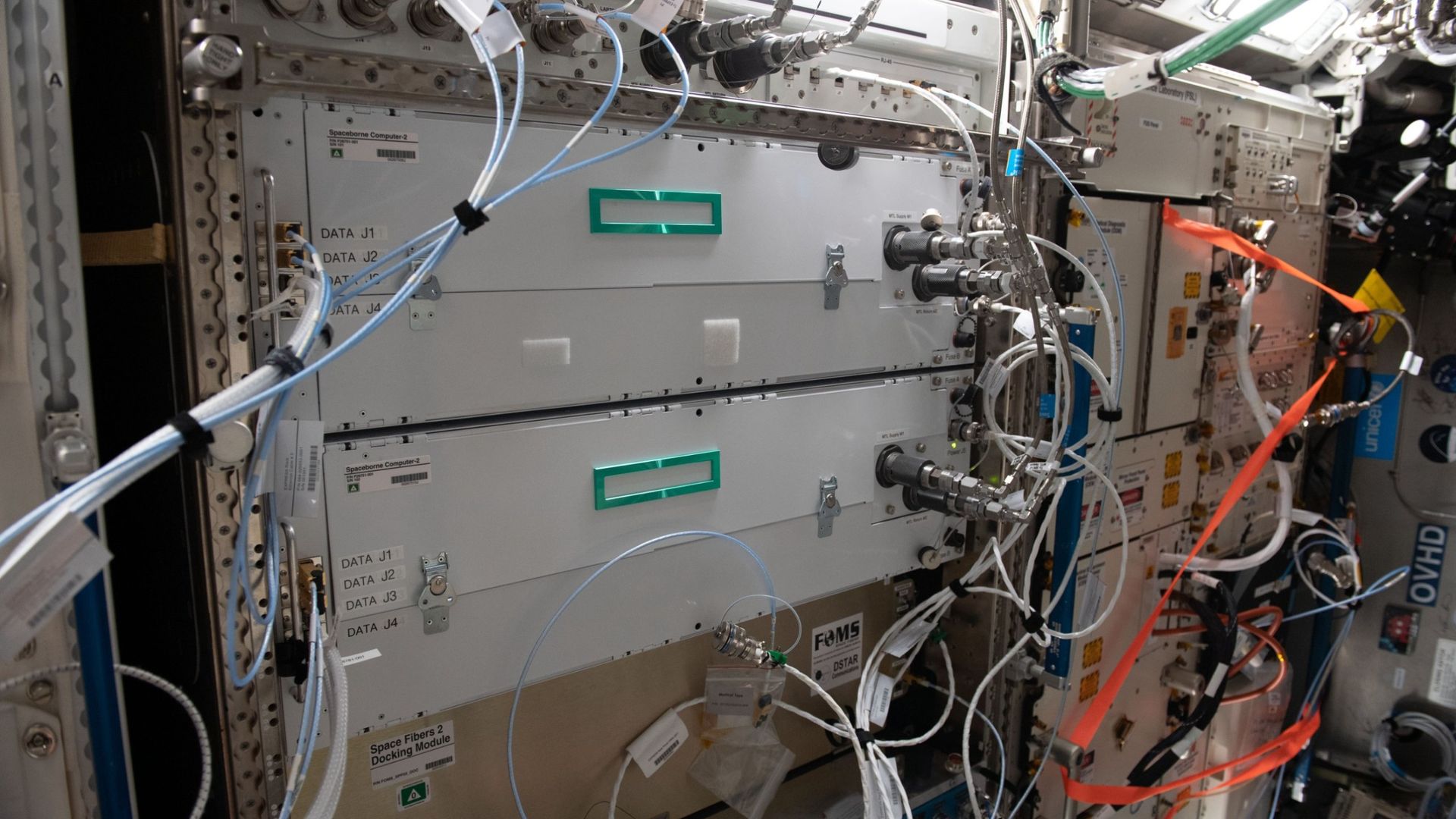
The original Spaceborne Computer launched in August 2017 on SpaceX’s CRS-12 to the ISS. It also ran HPL with HPCG, surpassing one teraflop, according to HPE. It was rack-installed and water-cooled; the fanless Computer-4 is quite miniaturized in comparison to the 124-pound original Spaceborne Computer. Spaceborne Computer-2, also on the ISS, is made of HPE Edgeline and ProLiant systems with Kioxia SSDs.

Two HPE Spaceborne Computer-2 units mounted in an equipment rack aboard the International Space Station, surrounded by cables.

(Image credit: NASA)

NASA will use the opportunity to run its Federated Learning for Unbounded and Intelligent Decentralization (FLUID) AI neural network, trained on data from the Earth, the Moon, and the ISS, coordinating three distinct models. The agency will also test a tuned LLM for semantic processing for handling onboard documents. Deloitte, for its part, will test its Silent Shield, “a new system to detect cyber intrusions” with near-real-time predictive analytics. Testing ideally occurs onboard, as the link to Earth is slow with low levels of bandwidth, Follett explained.

The launch is planned for the fourth quarter of 2026, using a SpaceX Falcon Heavy launch vehicle, SpacePolicyOnline reports. It will take several days for the lander to reach the Moon and its surface. The FLIP rover is designed to operate for one lunar day, or about 14 Earth days, before attempting to survive the night via hibernation, Follett said, making for a relatively tight benchmarking window.

  •  

Four workers killed after fall at TSMC’s 2nm fab construction site

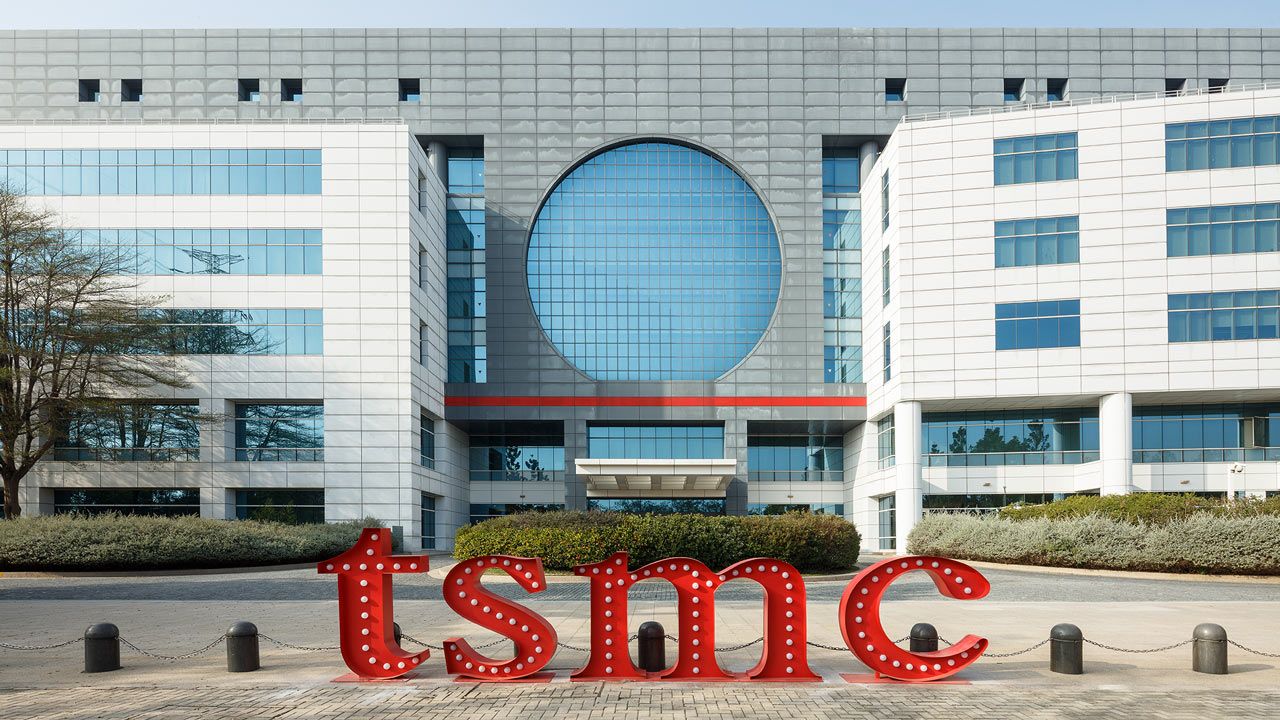
Three contract workers died, and one more is in intensive care after an accident at the construction site for TSMC’s 2nm Fab 22 in Kaohsiung, Taiwan, reports Taiwan’s Central News Agency. The Southern Taiwan Science Park (STSP) Bureau suspects the cause was a broken bolt on a steel connection plate that sent the workers and steel components tumbling. Steel hoisting on the project has been halted, and the STSP has sent labor inspectors to investigate. The accident is not the first of its kind but rather follows at least a half dozen others since September 2024 at TSMC construction sites in Taiwan, according to local reports. Each of those earlier accidents killed one worker.

Local police said that the men were welding a steel beam on an upper floor and fell with it, while the STSP said the workers were performing steel-structure hoisting and installation when a third-floor connection-plate bolt apparently broke.

10 emergency vehicles were sent to the site with 22 personnel, and all four men involved in the incident were taken to the hospital. On-site medical staff gave first aid, but three of the workers died despite resuscitation efforts, and the fourth was moved to intensive care. The workers were employed by a contractor working on the fourth phase of the complex’s construction, and TSMC said the area was within that contractor’s scope of work.

According to the report, TSMC stopped the related construction work on its own and is working with authorities and supervising the subcontractor’s follow-up.

The Fab 22 complex, located in Kaohsiung’s Nanzi District, is part of the science park and is being built to accelerate 2nm manufacturing. TSMC entered high-volume 2nm, or N2, manufacturing in the fourth quarter of 2025, including at Fab 22. The complex has five phases planned, with a total investment TSMC puts at more than NT$1.5 trillion, or about $46 billion. The accident happened on the construction side, not in a producing fab. Kaohsiung’s deputy mayor said construction on Phase 4 began in August 2025, with operations expected in the fourth quarter of 2027.

Business Today reports that TSMC fab construction has increased, from four fabs a year in 2017–2024 to nine a year in 2025 and 2026. The deaths come as the company plans for 13 new leading-edge and advanced-packaging fabs in Taiwan, with company-wide capex of $60 billion to $64 billion this year.

The faster pace has encouraged the addition of a contractor’s safety record as a weight in selection and a plan for a Taiwan Semiconductor Construction Engineering Safety Association with construction partners. TSMC Chairman C.C. Wei said at last year’s shareholders meeting that safety cannot be compromised, and the company’s 2025 annual report said it will keep investing in fabs across several locations in Taiwan “with a strong emphasis on construction site safety.”

Cliff Hou, TSMC senior vice president and deputy co-COO, told Business Today that increased worker count and overlapping construction have raised the risk, requiring careful supervision, and that TSMC’s contractor lost-time injury rate had fallen about 42% from last year’s high as of late May, when the publication toured the Nanzi site to see the overhaul. It’s too early to call the program a failure, with the cause as yet unknown.

The accident comes less than a week after an explosion killed two people at Intel’s chip plant in Israel, though that was an operating fab rather than a construction site. Both accidents come as chipmakers race to meet demand, with global chip sales passing $1 trillion through August, according to the Semiconductor Industry Association.

The STSP’s findings will determine what penalties, if any, will fall under Taiwan’s Occupational Safety and Health Act, while it assists the victims’ families. No date has been given at this time for that or for the Phase 4 steel hoisting restart. Nor has TSMC commented on any schedule impact.

  •  

Jensen Huang Nvidia GTC keynote disrupted by Greenpeace protest over chips in Russian drones

Protesters disrupted Jensen Huang's Nvidia GTC keynote in Berlin on Wednesday morning. Just minutes into the CEO's customary address, the broadcast was interrupted by a heckler from the crowd demanding the CEO answer claims that the company's chips were found inside Russian drones, and charges of environmental destruction more broadly. While the incident wasn't fully picked up by Nvidia's livestream, footage filmed by attendees shows protestors standing on chairs with a large banner that reads "Nvidia, clean up your dirty business!"

Multiple videos and images shared to X show protestors brandishing a large banner with a Greenpeace logo. "Jensen, what about the technology that was found in Russian drones? Those were Nvidia chips. What are you doing about that?" one of the protestors called out across the auditorium. "What are you doing about that? What are you doing about the environmental destruction?" the heckler demanded.

GTC Keynote disrupted by protestors. What looks like @Greenpeace #GTC #GTCBerlin https://t.co/LqSdpmQLi0October 21, 2026

Huang can be heard on the broadcast and in the video stating, "It's okay, go easy," as security rushed to escort the protesters out of the hall. "I'll talk to you later," Huang stated as the individuals were removed from the premises.

The complaint raised by the protester appears to relate to recent reports that Nvidia Jetson chips have been found in Russian cruise missiles used against Ukraine, as well as in AI drones. Reports indicate Russia's S-71 'Monochrome' weapon has autonomous targeting capability powered by Nvidia's consumer-grade Jetson Orin chip. "Our Jetson Orin modules are consumer-grade products sold to students, developers, and startups for a wide range of beneficial applications," Nvidia told Tom's Hardware at the time. The company reiterated that the chips are not available in Russia and are not designed for military purposes, but admitted it cannot track the resale of pre-owned Jetson chips after they are sold.

A report in August claimed that a Russian AI drone killed three civilians in Ukraine, the first documented case of civilian deaths caused by a Russian drone using fully autonomous targeting. Images of the recovered drones confirmed they contained Jetson Orin modules. "All important issues, but let me get through my keynote," Huang quipped before continuing his presentation.

Huang is in Berlin for Nvidia's three-day GTC event, taking place from October 20-22. The customary keynote, given this morning, also includes fireside chats and talks for developers and business leaders.

  •  

Apple’s 2026 Designers of Tomorrow Explores Creativity Beyond the Screen

Apple’s 2026 Designers of Tomorrow exhibition opened October 20 at Hôtel de Maisons in Paris. Returning for a second year in collaboration with Design Miami, the showcase is curated by Rodman Primack and organized around the theme of presence. A similar exchange between digital exploration and physical production appears in Bünyamin Aydın’s work with iPad Pro for Les Benjamins, where sketches and shared references helped develop a fashion collection.

The featured participants are Salem S. Charabi, Isabel Rower, Yoonjeong Lee, and Parafernalia. Their work provides a starting point for examining a broader creative question: how can an object encourage someone to stop, pay attention, and engage with their surroundings?

For Apple readers, the exhibition also offers a different way to think about creative technology. The finished works invite attention through their materials and use, while digital tools operate behind the scenes.

Four Projects With Different Material Languages

Charabi’s The Eminence of Light combines palm fronds, banana paper, and limestone in a lantern developed with MacBook Pro sketching and 3D modeling.

Rower’s Padded Chair 1860 features a glossy finish and ceramic beaded fringe that makes sound when brushed. Her workflow includes documenting ideas on iPhone and arranging references in Keynote.

Lee’s New Form combines a wooden table and lamp, incorporating worn pencils and approximately 5,000 layers of veneer. She uses iPad Pro and Apple Pencil within a connected workflow.

Parafernalia’s Genki Matsumura and Sebastián Zorrilla created MonoAmbiente 1, a stainless steel piece that opens to reveal stools and a table. Their geographically separated collaboration involves shared sketches and communication apps. Apple describes the projects and their development in its exhibition announcement.

A hand uses a digital stylus to draw pencil sketches on an Apple tablet screen, which displays a drawing app toolbar for designers of tomorrow.
Image Credit: Apple Inc.

Presence Begins With What an Object Asks You to Notice

Together, the projects suggest several ways to interpret presence. Light can draw attention across a room. An unexpected sound can make a familiar action feel different. A recognizable material placed in an unfamiliar role can prompt a second look.

These are useful distinctions because attention is not always a matter of visual impact. An object may become interesting through movement, proximity, or participation. Looking at a photograph and encountering the work physically can therefore produce different experiences.

That is an editorial reading of the exhibition’s theme, rather than a measured finding about visitors. Whether a particular piece creates that response will depend on the person encountering it and the circumstances of the encounter.

Digital Planning Supports Physical Judgment

The workflows offer a practical reminder that creative work contains several different kinds of decisions. Sketching helps establish a possibility. Modeling can help examine relationships between components. Collecting references provides material for comparison.

None of those steps eliminates the need to make judgments about the finished object. A convincing image cannot, by itself, establish whether a surface feels right, a structure behaves as intended, or an interaction is satisfying.

For someone developing a personal project, the useful question is which stage needs support. A student organizing visual research may need a clearer reference archive. Two collaborators may need a more consistent way to exchange revisions. A maker exploring a complex form may benefit from investigating its geometry before committing materials.

The exhibition illustrates specific workflows, rather than prescribing one equipment list for every creative discipline.

A designer with short hair wearing a black sweater stands in a studio next to a marbled ceramic vessel.
Image Credit: Apple Inc.

Collaboration Is Part of the Design Process

Working with another person introduces a separate challenge: making an unfinished thought understandable. A sketch that feels obvious to its creator may leave a collaborator unsure about scale, construction, or purpose.

A useful shared reference gives both people something concrete to discuss. It can expose disagreements early, preserve an alternative worth revisiting, or clarify which version is currently under consideration.

For readers, that offers an approachable lesson without requiring a professional studio. Naming revisions clearly, recording why a decision changed, and keeping references accessible can make a small project easier to develop. The value comes from the working habit as much as the software involved.

Read the Showcase as a Set of Creative Examples

Apple positions the exhibition around its products’ role in design. That makes it a curated account with a clear commercial perspective, rather than an independent comparison of creative platforms. The featured experiences show how these designers work; they do not establish that equivalent results require identical devices.

The stronger takeaway is to examine the path from observation to finished object. Each stage needs a purpose: capturing something worth exploring, testing a possibility, communicating a revision, or assessing the physical result. For readers interested in making things, that process is the most useful part of the showcase—and something they can apply to their next project.

A Designer of Tomorrow uses an Apple stylus on a tablet screen to edit a digital illustration of a piece of furniture.
Image Credit: Apple Inc.

The post Apple’s 2026 Designers of Tomorrow Explores Creativity Beyond the Screen appeared first on AppleMagazine.

  •  

Inside the U.S. Suppliers Behind iPhone Duo and iPhone 18 Pro

The titanium in iPhone Duo and the camera system in iPhone 18 Pro connect familiar product features to specialized American suppliers. Behind those parts are different kinds of manufacturing: processing metal, producing advanced films, forming protective glass and fabricating miniature lasers.

Apple’s October 20 supplier announcement identifies several of these connections. Read alongside the manufacturers’ own documentation, it provides a partial map of the work behind the devices, rather than a complete account of their global production.

Apple’s broader U.S. manufacturing program brings together businesses with very different specialties. Following individual components reveals how a metal producer, a materials company, a glassmaker and a semiconductor manufacturer contribute to devices sold under the same brand.

Two hands holding smartphones—an iPhone 18 Pro Max vs iPhone 17 Pro Max—each featuring curved abstract patterns on their screens. The left phone, likely the newer iPhone 18, has a pinkish hue, while the right phone displays a dark gray design. Both are set against a plain light background.
Image Credit: Apple Inc.

Perryman Processes Titanium for iPhone Duo

Apple identifies Perryman as a titanium supplier for iPhone Duo. The relationship concerns material production; it does not establish that Perryman builds the finished enclosure, hinge or assembled phone.

The geography requires care. Apple’s release groups melting, forging and rolling at Houston, Pennsylvania. Perryman’s facility directory describes a distributed network: melting and ingot breakdown at Coal Center, hot rolling and much finishing at Houston, and intermediate processing at Frackville.

Perryman’s operations therefore span several Pennsylvania locations. Apple has not published a facility-by-facility production route for its titanium orders, so the company’s broader manufacturing network provides context rather than a confirmed itinerary for each iPhone component.

Perryman lists electron-beam and vacuum-arc melting equipment, followed by processes that turn ingots into semifinished and finished material. It also documents laboratory and nondestructive testing capabilities.

In practical terms, the work converts raw inputs into controlled material forms that other manufacturing operations can use. Consistency in composition, dimensions and internal quality matters before a supplier further down the chain shapes a consumer product.

suppliers - Close-up of a detailed, miniature landscape resembling arched rock formations or cave entrances, with textured surfaces and fine dust or sand—crafted using 3D printing techniques—in grayscale tones.
The Ultra 3’s titanium imprint process creates a clean, sculpted finish around its iconic contours.

Qnity Supplies Films for the Variable Aperture

Qnity Electronics has a different role: Apple says it will produce advanced films essential to the iPhone 18 Pro’s variable-aperture camera system.

An aperture controls the opening through which light enters the camera. Changing that opening helps manage exposure and depth of field, meaning how much of a scene appears acceptably sharp.

The announcement links Qnity to materials supporting that system, rather than identifying it as the manufacturer of the entire camera. Apple does not disclose the films’ composition, their exact position within the assembly or the production process.

It also does not name the relevant factory. Delaware is Qnity’s headquarters location, not sufficient evidence of where these particular films are made.

Qnity’s role highlights a less visible side of camera development: the materials that support a mechanism can be as specialized as its optical and electronic components. Apple identifies the films’ connection to variable aperture, but leaves their precise engineering role undisclosed.

Corning Makes Protective Glass in Kentucky

Corning’s Harrodsburg, Kentucky, operation supplies specialty glass for Apple, including Ceramic Shield. Apple’s October announcement sets an end-of-2026 target for all iPhone and Apple Watch cover glass, including iPhone Duo, to come from that facility.

Harrodsburg is already operating; the broader production transition remains a dated target. Corning’s account of the plant describes both current manufacturing and development work for future products.

Opened in 1952, Harrodsburg is Corning’s longest-running American plant. Its history includes the development of fusion-draw glassmaking, a process used to create large, thin sheets of glass. Corning describes the site as both a manufacturing operation and a place where teams develop materials for future products.

Protective cover glass is distinct from the panel that generates an image. Manufacturing a transparent protective surface involves different requirements from producing OLED pixels, electronics or the other layers in a display assembly.

The iPhone Duo connection therefore should not be expanded into a claim that Corning supplies its complete folding display. Apple’s statement identifies cover glass, with a specific production goal.

Three stacked smartphones—resembling the iPhone 18—display music controls for “the bridge” by Kelela & PinkPantheress, with playback buttons and Dynamic Island notifications visible on each screen, all running the sleek new interface of iOS 27. The phones are a striking dark purple set against a deep black background.
Image Credit: Apple Inc.

Coherent Produces Lasers in Sherman, Texas

In an August 2025 supply announcement, Coherent identified its Sherman, Texas, facility as the production site for vertical-cavity surface-emitting lasers, or VCSELs, supplied to Apple under a multiyear agreement.

These semiconductor devices emit light from their surface. Coherent connects them to features including Face ID on iPhone and iPad; Apple’s latest announcement specifically associates its technology with iPhone 18 Pro.

Sherman has compound-semiconductor capabilities covering epitaxy, fabrication and device manufacturing. Epitaxy means growing controlled semiconductor layers; fabrication then creates the structures needed for individual devices. This is specialized chipmaking for optical functions, rather than assembly of a complete camera.

The connection described here concerns Face ID and supported Apple devices, with the October announcement specifically naming iPhone 18 Pro. It illustrates why the supplier map differs by model: a component associated with one phone should not automatically be assigned to another.

Different Processes Contribute to One Device

These suppliers illustrate distinct stages of production. Metal processing prepares structural material; films support a camera mechanism; cover glass protects surfaces; semiconductor lasers contribute to optical sensing. Each requires its own equipment, expertise and quality checks.

Their contributions establish specific American manufacturing connections, not U.S. final assembly or an entirely domestic iPhone. Following the component and its documented production stage provides a more accurate picture than treating every supplier announcement as evidence that the whole device is made in one country.

Two hands hold different devices: one, an A20 Pro folded phone showing a spiral staircase; the other, a tablet displaying a person walking in a red, sunlit corridor with an arched glass ceiling. Both screens feature vibrant architectural scenes.
Image Credit: Apple Inc.

The post Inside the U.S. Suppliers Behind iPhone Duo and iPhone 18 Pro appeared first on AppleMagazine.

  •  

U.S. Army developing program that would deploy AI agents to autonomously seek and destroy targets in enemy digital infrastructures

The U.S. Army is allegedly developing a program to deploy autonomous AI agents that can navigate digital and network infrastructures, identify targets, and “neutralize” them. According to an Oct. 19 report by The Intercept, citing leaked official documents from the Army Cyber Command (ARCYBER), the nascent program, codenamed “ECHOTRIBBLE,” is primarily focused on offensive missions with the goal of neutralizing targets by “disabling the threat completely or temporarily, deleting the threat from the target.”

The program purportedly seeks to develop modular, autonomous AI agents that would function like computer worms, stealthily navigating adversary networks, moving between devices, and self-replicating across different operating systems. The agents would operate lightly in contested cloud environments and air-gapped systems alike, keeping reports minimal and concealing any required transmissions. Once an agent identifies and neutralizes a target, it would self-destruct, ideally without alerting the target or leaving any traces of its existence.

Cybersecurity experts have raised safety concerns about the project. A recent string of events has seen AI agents escape their environments and autonomously execute unassigned tasks. The document says the army will implement “predefined triggers” to help agents precisely distinguish targets. However, experts worry that if agents designed for benign tasks could execute unplanned, sometimes dangerous, actions to achieve those tasks, what should be expected of self-replicating agents designed specifically for offensive missions? Anthropic’s experiments showed AI agents can set up inference on different hardware and replicate across a network.

The Army also wants the agents to be capable of “Self-Directed Behavior,” acting with as little human oversight as possible, as this is necessary to achieve the desired level of autonomy. Conversely, this level of autonomy has seen AI agents bypass guardrails to complete their tasks. Government intelligence agencies have also been known to penetrate target networks through civilian infrastructure. “The target may well be hit. But what path will it take?” asked Hyrum Anderson, co-founder and CEO of the AI security firm Abundant, as quoted by The Intercept. “Will it go through a U.S. water utility on its way, because that’s where the adversary has staged its command and control, and take that down too?”

Another angle of concern is how the agents would make judgment calls. While AI agents are excellent at overcoming obstacles in their path, there's no predicting with 100% accuracy what they would consider obstacles or what path they would take to overcome them. “One of the reasons that we trust 19-year-old Marine corporals in Ramadi with live rounds and a weapon is because they have both the compute substrate — the brain and the eyes — but the deep world knowledge to understand, ‘Yeah, I probably shouldn’t do that,’” said William Marcellino, a senior behavioral scientist at the RAND Corporation researching military AI applications. “That is not something that current public AI technology has.”

The ECHOTRIBBLE program is in the early prototyping and industry assessment phase and is led by ARCYBER, the Army Cyber Technology and Innovation Center (ArCTIC), and the Cyber Fusion Innovation Center (CFIC), with private vendors and academic researchers proposing and designing the software. ARCYBER and ArCTIC dictate the operational requirements and rules of engagement, while CFIC, a defense non-profit organization, acts as an intermediary between the Army and commercial tech companies. The Army recently held a virtual Assessment Event from October 6 to October 8, 2026, where it evaluated 65 technical whitepapers submitted by private vendors proposing solutions for the agentic framework and narrowed them to five. The final candidate(s) will be issued funding and formal prototype contracts.

  •  

US restarts three shut-down nuclear reactors to feed AI data centers

The current and expected power draw of AI data centers has been the subject of strong discussion, but today, there appears to be some good news. Three U.S. nuclear reactors are being restarted after many years offline, expected to bring 2.25 GW total to the grid. According to a report, the Palisades Nuclear Plant in Michigan, the Crane Clean Energy Center on Three Mile Island (Pennsylvania), and the Duane Arnold Energy Center in Iowa are getting a fresh set of proverbial tires to get rolling again.

The Palisades plant was under active decommissioning, apparently marking this event as the first time a nuclear reactor is being put back to work after dismantling had begun. Despite what sounds like a tough starting point, this plant is the one that's furthest along, as it was loading fuel in August 2026 and is expected to generate 800 MW around March 2027.

Much like the other projects mentioned here, the Holtec Palisades firm running the reactor took a loan from the U.S. Department of Energy. Palisades borrowed from the DoE under the Biden administration's 2024 investment in nuclear energy, while the others were issued under the purview of the Trump administration's 2025 push.

The second reactor is the Crane Clean Energy Center on Pennsylvania's Three Mile Island, repurposing the facility's Unit 1. The project started in 2024, with Constellation Energy saying it would spend $1.6 billion total for the reactor. The firm then took a $1 billion loan from the Department of Energy in 2025. Microsoft is set to be the main customer, with a 20-year contract. This facility is projected to bring 835 MW online sometime in 2027.

This facility was famous in 1979 for the partial meltdown of its Unit 2, although mercifully the event had relatively tame environmental consequences. Constellation's ongoing project is restoring and refurbishing Unit 1, which didn't show significant issues until its 2019 decommissioning and has undergone a safety inspection from the Nuclear Regulatory Commission. This entity still needs to grant its blessing before the reactor starts loading fuel.

The Duane Arnold Energy Center in Iowa is the third unit being brought back to the grid, in a collaboration between NextEra Energy and Google. The predicted output is 615 MW, with the juice expected to start flowing in 2029. Next Energy CEO John Ketchum stated that the firm was happy with its cooperation contract with Google, as it meant that "none of the costs are being paid by residential customers in Iowa."

All three facilities had previously been shut down at various points as they were deemed too expensive to run, as labor and maintenance costs made nuclear-generated watts pricier than alternative means of production.

But the financial landscape for power has shifted, plus with such overwhelming demand and grid connections being a primary blocker for data center buildouts, their operators are likely willing to pay for premium power as long as they get it now instead of in a few decades.

Some quick browsing indicates that Michigan is going to need somewhere between 1.2 and 2.3 GW for data centers alone around 2030. Pennsylvania's forecast has a wide range of 0.8 to 3.4 GW, while Iowa's range is 1.55 to 2.8 GW. These figures are loose, as they include planned capacity for data center projects that may or may not end up being built, and whose timetables may slip due to economic conditions, hardware availability, and public resistance against expansive buildouts.

  •  

Modern software is built on the backs of low-paid maintainers, opening the door to potential threats

Modern computing systems and devices typically require pieces of crucial open-source software, typically maintained by unpaid or low-paid volunteers. Recently, a report collated a list of critical open-source projects, noting which of them are chronically underfunded and/or understaffed. The information is sobering: 11 out of 23 of the listed projects currently only have one or two maintainers, and funding is generally scarce and sometimes nonexistent.

The Data Drop's report on open-source maintainers identifies that having only one or two sets of eyes on critical pieces of software means that sooner or later something breaks — and it tends to do so in spectacular fashion, given its ubiquity. So, what happens when these projects, which are widely used across software, go underfunded or understaffed?

Lessons from the past

In 2014, the same year as Heartbleed, Shellshock made waves: a vulnerability in the Bash shell that's present in Linux, macOS, and Unix-type systems. The problem was traced back to a line of code present since 1989, displaying how even software that's thought to have all the bugs hammered out of it can still fall prey to attacks. A quick look at Bash's commit history shows it's almost exclusively maintained by Chet Ramey.

In 2016, ImageMagick was exploited, providing attackers with remote code execution. This library is used for image manipulation across a wide range of software, in webpages, mobile apps, and more. A 2020 analysis revealed that hundreds of security issues had been found over the years in its extensive codebase. Nearly every code contribution in the past couple of years has been done by an individual named Dirk Lemstra.

Contemporary examples include 2021's Log4Shell exploit, a critical vulnerability in the Apache Log4j logging library used in millions of servers. The libwebp image-handling library saw a zero-day vulnerability in 2023, and the xz compression library used across Linux and iOS was compromised in 2024.

Thankless work

Key points in the report mention specific repos, which might be under threat. Somewhat unsurprisingly, the low number of overall maintainers and the unpaid nature of the work make it unattractive to perform.

The main time-zone file used across Linux-based operating systems is maintained pro bono by Paul Eggert, a UCLA teacher. Core-js, a piece of support software that lets new JavaScript work in old browsers and is estimated by the author to be used in half of the busiest websites in the world, is handled by Denis Pushkarev. He once had to endure criticism from the community because he added a command-line message to the library's installer asking for help or a job.

The HarfBuzz library developed by Behdad Esfahbod is a cornerstone in ligatures and text shaping in Middle Eastern languages. In those writings, a letter changes shape and/or orientation according to what's around it. Esfahbod handles that vast majority of the project's code, and doesn't mention public or corporate funding.

Libjpeg-turbo handles JPEG images on Android, Firefox, LibreOffice, and every Chromium-based browser. It's kept ship-shape by D.R. Commander aka DRC, who occasionally is contracted for library-specific work, though at arguably modest values of "3-4 figures rather than 6 or 7." Libxml2, just like the label says, handles XML reading and writing across numerous applications and operating systems. Nick Wellnhofer, the original maintainer, stepped down in September 2025, after years of work with little income.

The SQLite project provides a one-file database that's exceedingly easy to integrate into most software, instead of complicated, resource-heavy databases, while still retaining standard SQL language and accouterments. Thanks to its ease of use, it found its way into an astonishing number of applications. Examples include WhatsApp, Dropbox, Android, Windows, and all major browsers.

The project estimates that there are about a trillion instances of SQLite in use. Just four people keep this critical project together, and they've gone to the length of removing their names and photos from the project's page, as "there are a lot of crazy people in the world who might misuse that information." The project is funded by the offering paid support via the founder's company, though there's no word on effective income, especially when it presumably needs to feed four mouths.

Funding is there, but scarce

It's not all doom and gloom, though. Take curl (the software), for example. Almost every developer has used it, thanks to its URL-fetching abilities and extensive scripting options. The project was started by Daniel Stenberg, who is now paid to work full-time on it. The team has now grown to 11 and has received funding through Open Collective and Germany's Sovereign Tech Agency, among others.

Likely due to the lessons learned from their past respective debacles, both the Log4j and OpenSSL projects are likewise funded by the Sovereign Tech Agency, as are the FFmpeg video file handler and the OpenSSH secure shell software that's ubiquitous in Linux servers.

All things considered, it's easy to argue that the critical importance of all the aforementioned software merits sizable investments from industry players, especially those whose commercial products benefit the most from the community's efforts. Plus, even if the firms feel no moral obligation to contribute, in the day and age where AI agents are finding exploitable vulnerabilities in hours, donations to these open-source projects could also be considered investments.

  •  

Intel asks FCC for waiver to buy foreign robots

Intel has asked the Federal Communications Commission (FCC) to make an exception for the automated guided vehicles (AGVs) that the company uses to transport the sensitive silicon wafers and other materials, containers, and supplies needed to make the most advanced chips in its fabs. According to Bloomberg, the American chipmaker fears that its AGVs would fall under the blanket prohibition against foreign-made robots after they were added to the FCC’s Covered List.

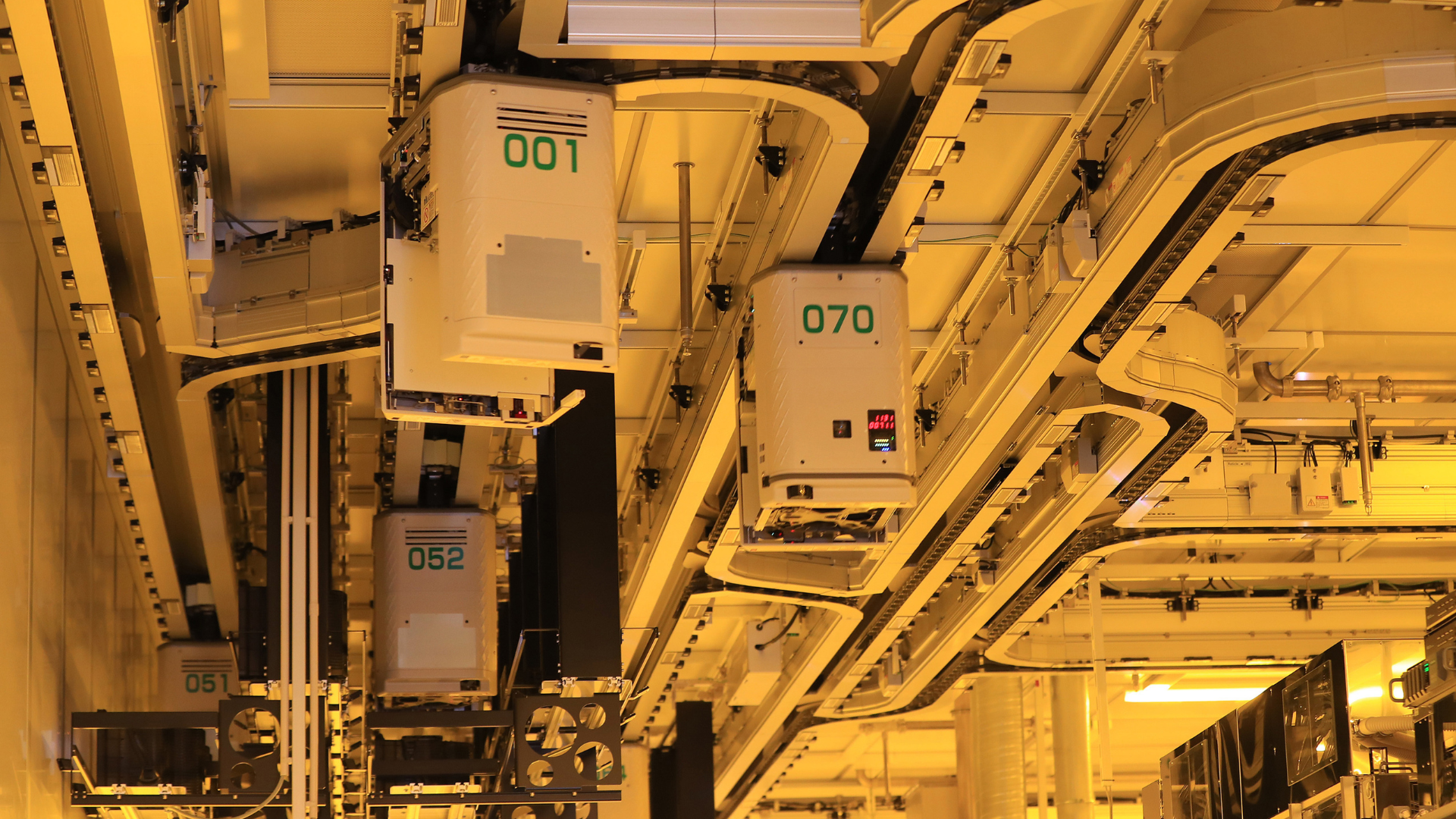
AGVs are niche machines that chip fabs use to transport materials and supplies between tools and sections of the fab, helping ensure that the cleanroom conditions required for each manufacturing process are maintained. This makes them critical equipment for U.S. semiconductor manufacturing, but, apparently, there are no suitable domestic alternatives for these devices at the moment. Intel’s current fleet of AGVs requires continuous maintenance, including software and firmware updates, and if it’s forced to find a local supplier for its AGVs, the company says that it would take years, crippling the United States’ chipmaking efforts.

The biggest AGV suppliers are Japanese companies like Murata Machinery and Daifuku Co., while a few smaller businesses from South Korea and Taiwan are also trying to break into the market. It’s unclear why these companies haven’t applied for a conditional approval yet, which would allow them to continue selling these products in the U.S. while also promising Washington that they’ll set up a manufacturing base in the country. This is something that Netgear has already done, allowing it to continue selling its foreign-made routers despite being an American company.

Intel says that it remains unclear if updates to its AGVs would break compliance with the FCC, and that it’s asking the agency to issue a conditional waiver “out of an abundance of caution to ensure the ongoing operation of these specific AGV units.” While Team Blue is the only company concerned about AGVs at the moment, other chip manufacturers would likely need a similar waiver in the near future, especially as they build more fabs in the U.S. This includes TSMC, which is planning to build 12 more fabs and four packaging facilities in Arizona, Samsung, with its new Taylor, Texas, fab, and even Elon Musk’s Terafab, which has already begun construction.

Washington has been using the FCC to force companies to invest in American manufacturing. Its blanket bans on foreign-made products like drones and routers have affected some of the biggest brands in the U.S., including DJI and TP-Link. While these bans do not outright ban the sale of all products made by these companies, especially those that have already been approved before, they make it impossible for them to introduce new products and even release software updates to their existing product line. The FCC eventually walked back on the software update ban, but they still would not be able to register new products unless they build them in the U.S.

  •  

Chinese crime ring steals more than $5 million in gift cards from Staples customer service

Millions of dollars worth of gift cards were stolen and then used to buy high-value tech gear at retailers like Target, Sephora, and Lowe's after a Chinese crime ring gained access to an internal Staples system and then used it to issue more than 15,000 cards to itself. While the hack hasn't been made public to date, a 404 Media report notes that it actually took place back in 2023.

The outlet reviewed court records that show that Homeland Security Investigations (HSI) was told about the hack in October of that year. The hack came to light after it led to a search warrant that was unsealed last week. And while the document doesn't specifically name Staples as the victim of the hack, 404 Media has confirmed that it was the company affected based on other information. Such information includes the fact that the victim company is headquartered in Massachusetts, that it uses Blackhawk Networks to fulfill gift card orders, and that the company uses an internal customer support system called Nexus. The report notes that a reference to Nexus can be found on a former Staples executive's LinkedIn profile.

While Staples was under the impression that Nexus could not be accessed from beyond its own network, hackers found that not to be the case. They then "performed multiple heap dump requests," a process that captures all of the data held in an app's memory. That information gave the hackers the tools they needed to hijack logged-in sessions of Staples customer service employees. From there, they were able to issue gift cards at will.

Once the gift cards had been issued, the crime group sent runners to physical retail stores to spend them before they were identified and canceled. Target found that 35 gift cards were used at a New Hampshire store, with high-value products from Apple, Bose, and Beats all bought. All 35 cards were used within a period of just a single hour, although not all of them were obtained via this hack.

In total, Target told investigators that 3,850 gift cards worth over $140,000 were used across 85 different stores in just two days. Sephora was hit for $58,600 worth of sales, while Lowe's saw $226,000 spent across online and in-store purchases. In total, 4,630 stolen gift cards were used with a value of around $425,000.

This hack was just the tip of the iceberg, too. Last April, a Department of Justice announcement confirmed that three Chinese nationals had been sentenced for their part in a gift card fraud conspiracy. Including the Staples hack, the crime group stole more than $100 million worth of gift cards.

Chinese organized crime groups often pop up on the radar of U.S.-based law enforcement. Earlier this year, a Chinese phishing service that was used to generate scam websites using AI was dismantled. The service was linked to almost $2 billion in losses.

Google Preferred Source

  •  

Google DeepMind claims four AI agents beat Minecraft in 27 hours by writing 2,783 programs of their own

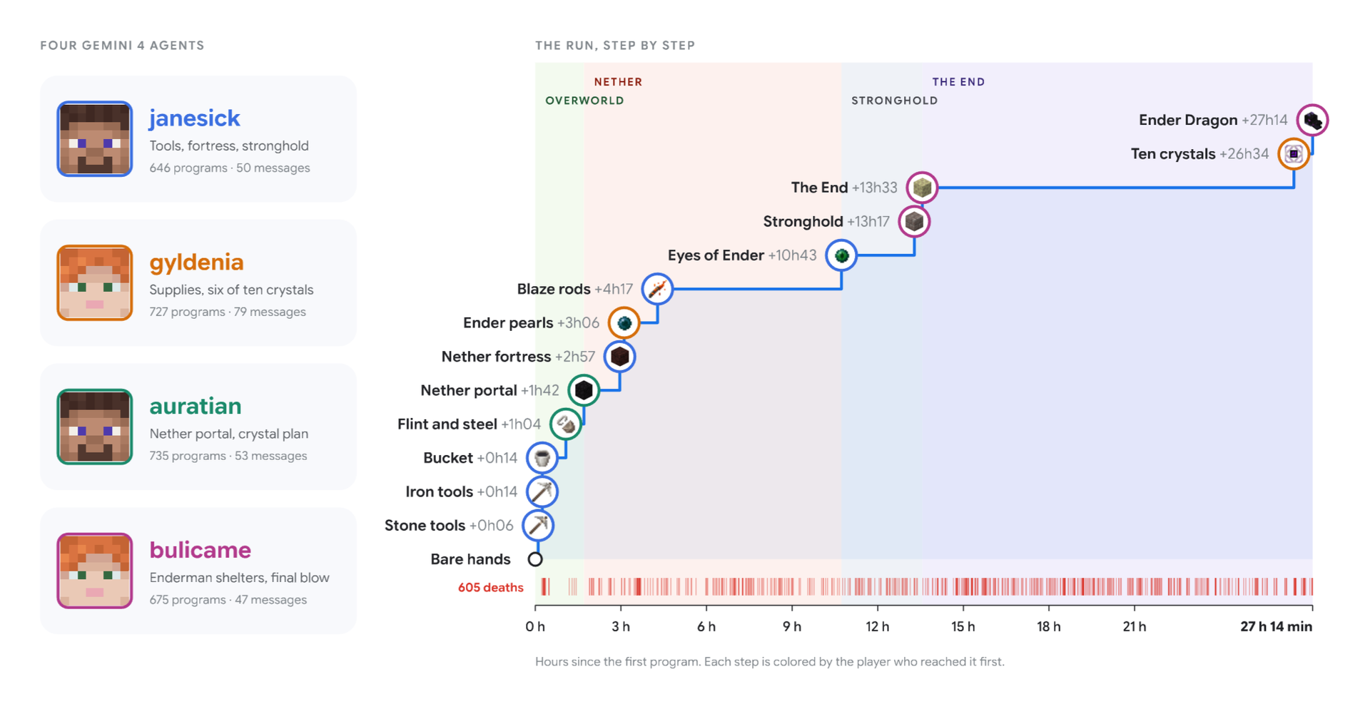
The game of Minecraft is no match for a team of four Gemini 4 Argon agents, as they were able to defeat it in 27 hours with 2,783 self-written programs, a paper from Google DeepMind reveals. The agents did die 605 times, even on Easy, and about half the run was spent fighting the Ender Dragon, the final boss of the game. The run finally came to completion when the End was solved by stacking dirt to reach the boss’s crystals, at an estimated cost of around $520 in tokens.

The experimental run was designed from the get-go with one goal: kill the Ender Dragon. The playthrough involved a random, shared survival world on Easy with four agents — a fifth agent existed only for reporting — from Gemini 4 Argon, Google’s latest frontier model. Each agent had its own player through the open-source Mineflayer JavaScript library for Minecraft bots, but they were able to coordinate through in-game chat and shared notes. Every program used in the run was written by the agents themselves, and the emphasis is on coding and teamwork rather than game-playing.

Google DeepMind chart of the four Gemini 4 agents, janesick, gyldenia, auratian and bulicame, beside a timeline of their Minecraft run from bare hands to the Ender Dragon over 27 hours and 14 minutes

(Image credit: Google DeepMind (Faldor et al.); textures: Pixel Perfection, XSSheep and Nova_Wostra, CC BY-SA 4.0)

The authors say this is the “first end-to-end autonomous completion of Minecraft by AI agents,” at least “to our knowledge,” qualified by the use of Mineflayer “without pre-scouted seeds or other game-specific tools written by humans.” Mineflayer tells the agents where blocks and creatures are, with a pathfinding plugin to plan routes. There was “no human input during the run” and “no one assigned roles or wrote game logic.” The run, starting with the first program and ending with the dragon's death, took 27 hours and 14 minutes.

Although the agents were not given roles, within about 10 minutes a division of labor was proposed in chat by bot janesick. Bot Auratian offered an alternative plan while Bot Gyldenia acknowledged it. The roles ended up being: Gyldenia for food, beds, and flint; Bulicame for diamonds; Janesick for iron and tools; Auratian for the Nether portal. Moments of losses, such as a Ghast fireball destroying dropped items, led the team to diagnose the cause and write rules to prevent it in the future.

Finding the stronghold involved janesick, who threw two Eyes of Ender from different spots and sampled each eye’s flight once every 50 ms, triangulating the location. Carrying the eyes involved its own dire moment when Auratian drowned during the task, but the spot was noted, and the eyes were rescued.

The eventual fight with the dragon led to 69 deaths, and the ten crystals kept regenerating the boss until Auratian discovered they could use dirt pillars to reach the crystals. Four hours and 40 minutes later, all ten crystals were downed, and the dragon was dead 39 minutes after that.

The agents operated by writing short JavaScript programs, almost 2,800 in total, with 42 helper functions kept alive between programs, while a Mineflayer bot ran them in the shared world. Text was returned with status data, not pictures. This is a shared approach to the non-screenshot GPT-6 Astra clear of the Orc starting zone in World of Warcraft earlier this month. AI agents playing games is an ongoing trend, with Pokémon Red probably being the most popular, a game defeated in multiple ways, including with a Jev decision model layer.

Minecraft has also been a popular target, and the authors admit this, highlighting two earlier community dragon kills: a planner with an action-selection model on a fixed speedrun seed in Peaceful mode, and a single Claude Opus 5 agent that used 37 ready-made, high-level tools on Normal, versus Mineflayer alone for the Gemini team. AI Bengineering’s Claude run, relying mostly on Opus 5 at high effort, took 3 hours and 56 minutes from start — “no human input after the prompt” — to kill with 388 tool calls and only one death. The cost in that case, at API-equivalent rates, was about $93.

Google’s Minecraft run, using Gemini 4 Argon’s 50% introductory pricing, which runs from initial API access that followed the model announcement through Nov. 30, cost more than half a grand; at normal pricing, that’s more than a grand. A GPT-6 Astra Portal run last month, which took about 24 hours, came in at $571 in tokens.

Google’s run took about 1.35 billion input tokens with 91% served from cache. About 24,000 model calls involved around 16 million output tokens, a quarter of them thinking. In total, if we’re also including the observer agent, the session would be estimated at $810, or $1,620 after the promotion, at list prices.

Each player is driven by a “general-purpose Gemini 4 Argon coding agent,” which is a fancy way of saying that it’s not specialized for Minecraft. Gemini 4 Argon itself is a frontier model for “real-world software engineering, enterprise knowledge work like legal and finance, and cybersecurity defense,” according to a company blog. With Minecraft, 22% of the agents’ programs ended in an error, with more than 600 deaths.

Although the model was used for a game here, the run was designed to show that Argon is capable of “complex, long-horizon workflows” for complex real-world tasks and agent coordination. Such long projects can involve decompiling a game back into source code, as we covered recently with a Modern Warfare 2 rebuild that now has 83% of its functions matching the original byte for byte.

  •  

Ukraine rescues wounded soldier using drone in daring 'world's first' UAV evacuation of a human

The Ukrainian military is claiming a world’s first after using an unmanned drone to rescue an injured soldier on the eastern Kharkiv front. Ukraine’s United24 news shared a video of the historic first. It also explained that the wounded infantryman was stuck in a heavily mined area, guarded by Russian kamikaze drones.

🔴 HISTORIC FIRST: Ukrainian forces completed the first-ever aerial evacuation of an injured soldier from the frontline using a drone.Soldiers from the 92nd Assault Brigade and 30th Mechanized Brigade used a heavy Gurzuf Defence hexacopter to rescue the wounded infantryman from a heavily mined area.October 19, 2026

The above video starts with the Ukrainian drone locating the soldier, callsign ‘Kostya,’ in enemy territory. Various media reports suggest he was 11 miles (18km) behind enemy lines, at the mercy of Russian kamikaze drones, and perilously located in a minefield. Traditional land-based rescue was therefore not possible, but Kostya bravely agreed to be part of the first-ever human drone-lift rescue plan.

After being located, the injured infantryman clipped himself into a harness. He said, “That’s it, we can take off,” when he was fully buckled into the rudimentary-looking harness. UAV operator, callsign ‘Black’ from the 20th Mechanized Battalion, 30th Infantry Brigade, then appeared in the video and explained: “We were constantly in touch with him."

Ukrainian drone rescue key facts:

  • Drone used: Gurzuf Defense hexacopter
  • Drone capable of carrying 130kg (~287 pounds)
  • Drone’s known range: it has previously transported 90kg (~198 pounds) loads up to 25km (16 miles)
  • Infantryman weight: 80kg (~176 pounds)
  • Rescue distance: 8km (11 miles)
  • Hazards: enemy kamikaze drones, mines, gravity, many more

Wounded soldier rescued using hexacopter drone

(Image credit: United24 news video)

Being in constant touch with the operations HQ would have been reassuring. However, the surrounding presence of a fleet of Ukrainian support drones, both kamikaze devices and UAVs with anti-drone nets, was probably most comforting.

Eventually dropping back into safe(r) territory, after what must have been an arduous, nerve-wracking journey, control said, “Congratulations, you’re on the ground,” to Kostya, as he touched down in a field. Then the control room erupted into applause. They got their man back safely, and he is now being treated and is in recovery.

UAV operator ‘Black’ was delighted with the concerted efforts that brought back this wounded soldier. “A lot of people were involved, and everything worked out for us,” he said. Importantly, this may be the start of a whole new system of personnel evacuations for wounded and/or stranded soldiers using drone technology, indicated brigade leader ‘Napalm’ toward the end of the video.

  •  

A Chinese hacker used AI agents to break into more than 100 company websites

A Chinese-speaking hacker has been observed using artificial intelligence (AI) agents to probe and then gain unauthorized access to more than 100 websites belonging to some extremely well-known companies. From Deere, the farming equipment manufacturer, to SharkNinja, the company behind beloved kitchen appliances, the agents were able to leverage exposed instances of Carin, an open-source AI-powered problem-solving platform that has proven popular among hackers, a Reuters report explains.

This is just the latest example of hackers turning to AI agents in an attempt to level up their attacks on unsuspecting companies and services. Snorre Fagerland, principal threat researcher at the cybersecurity company NorForge, spotted the hacker's antics when observing Carin instances that had been inadvertently exposed.

Fagerland was able to watch multiple hackers go about their business, but the Chinese-speaking hacker was the most prolific, the report says. They targeted businesses based in the United States, Canada, Australia, and Japanese e-commerce sites. Notably, the hacker didn't get into detail when commanding their legion of AI agents. Fewer than 100 Chinese characters were used, yet the agents had attempted ot break into more than 1,200 different websites as of the week ending October 18, 2026.

These agents weren't simply throwing everything at a wall and hoping it stuck, either. Security researcher Fagerland was "impressed" by some of the tactics that had been used. In one case, the AI agents scoured digital records to find infrastructure associated with their target, located a public-facing control panel, identified a weakness, and then leveraged it to force the execution of malicious commands, the Reuters report detailed. "It's ⁠not straightforward to come up with solutions like that," Fagerland told Reuters. "It's not script kiddie stuff."

Vitally, the approach of using AI agents in this way means that they can be given instructions and then left to their own devices. With no supervision required, those commanding the agents are free to turn their attention elsewhere. While SharkNinja told Reuters that the attack only impacted a site used for product support information, the rest of the AI-aided hackers had more luck. One of the hackers monitored by Gargerland stole credit card data, while another tried to steal from a cryptocurrency exchange — although it isn't clear whether they were successful.

Google Preferred Source

  •  

Norwegian undersea cable builder pitches 2,800-mile transatlantic data link between Canada and Europe to bypass the US

A Norwegian company building fiber networks and data centers across Europe is looking for a majority partner to help fund and build a transatlantic undersea cable that would connect Canada with Europe directly, bypassing the United States. The project follows worsening relations between Washington and Ottawa, with the Canadian government looking to reduce direct reliance on its immediate neighbor, Bloomberg reports.

Project Leif Erikson, if it goes ahead, would stretch more than 2,800 miles, starting at the southern tip of Norway and ending up at Happy Valley-Goose Bay in Canada's eastern province of Newfoundland and Labrador. From there, it would continue underground over Canadian territory, passing through Quebec before reaching Montreal.

According to Bulk's co-founder, Peder Nærbø, the link would be part of a "sovereign cable system" for Canada. The project was touted to investors at a global investors summit, arranged by the Canadian government, in September, where the project claimed to provide "direct, secure, high-capacity data transmission for AI, telecom and hyperscale markets."

Canadian Industry Minister Melanie Joy, meanwhile, met with Nærbø earlier this year, and although the department declined to comment on Leif Erikson itself, it told Bloomberg that security and resilience for Canada's infrastructure are "key priorities" for PM Mark Carney's government. Only a few undersea cables currently connect Canada without passing through the United States first, and none by a company owned by Canada. The biggest, called Topez, is owned by Google owner Alphabet and connects Canada with Japan.

As for Bulk, it has, up until now, laid more than 6,200 miles of cabling locally and at sea. Bulk's goal is to "unlock the Nordics' potential for... renewable energy to be utilized for digital infrastructure." Nærbø believes that "Canada lacks resilience" but "the game-changer was when the current situation with the U.S. escalated."

Leif Erikson has backers, according to the report, but the EU and Canada still need to plan and sign off on the project and its route. Additional financing will be needed to get started, too, with it expected to cost more than $620 million to build. Bulk itself has significant Canadian investment, with 65% of the company owned by a real estate subsidiary of Canada's Sun Life Financial Inc., with several Canadian pension funds also invested.

Leif Erikson is a project that Nærbø has sought to kickstart for the last five years without success. With geopolitical pressures and old alliances fraying, however, new opportunities for its development have given it steam. To that end, Canada and Europe intend to endorse a statement in Montreal on October 29 that the two will look for "the best way to enhance digital links between Europe, Canada and Asia through new subsea cable infrastructure."

It won't be without challenges, however, including a 1,180-mile underground route through Canada that'll require the backing of Indigenous communities. Meanwhile, other European efforts include an undersea cable project at the North Pole to link Europe with Asia to bypass Russia and the Middle East.

  •  
❌