Elon Musk says ASML and other critical semiconductor equipment suppliers have expedited shipments for the ambitious Terafab semiconductor manufacturing facility, supporting his aggressive timeline for the joint megaproject between Tesla and SpaceX. He made the announcement during a live broadcast of SpaceX's Q3 2026 earnings call on X yesterday, October 20. Musk also said the company is targeting volume chip production at the project's primary facility in Gibbons Creek, Texas, by the third or fourth quarter of 2028, emphasizing that the timeline is highly aspirational and carries "big error bars."
"These are very aggressive dates, and we're very appreciative of ASML and all of our other suppliers in accelerating equipment deliveries in order to achieve this outcome," said Musk, CEO of both companies behind Terafab. SpaceX plans to manufacture its first experimental test chip at its research fabrication facility in Austin, Texas, around Q2 2027.
Aside from Terafab, Musk also outlined near-term ambitions for his AI companies during the broadcast, saying he expects them to have 2.5 to 3 gigawatts (GW) of computing capacity active by the end of 2026. He also stated he is highly confident about bringing an incremental 10 GW online in 2027, saying he "would be surprised" if they do not hit a total of 13 GW of AI compute by the end of 2027.
Meanwhile, the next-largest project by planned capacity, the now-restructured 10 GW Project Stargate, was expected to reach full capacity in the 2030s. Meta's 5 GW Hyperion also has a similar timeline. To achieve the 13 GW milestone, Musk revealed that SpaceX and xAI are aggressively procuring upcoming next-generation NVIDIA architecture. He announced plans to get a massive 440,000-GPU Nvidia "Vera Rubin" training cluster online by the end of Q2 2027.
Shifting back to Terafab, Musk also boasted that once fully scaled and operational, the sheer commercial value of Terafab's advanced chip output will place it within the top 20 global country GDPs from a single physical building. For context, the 20th country on the list is Switzerland, with a GDP of around $1.14 trillion. The facility is a planned multi-billion-dollar, vertically integrated chip factory in Texas, with an ambitious goal of manufacturing 1 terawatt (TW) of AI computing power per year. Terafab will fabricate logic, memory, and advanced packaging internal architectures in one place. The project's massive planned output has mandated various collaborations across the semiconductor supply chain. Terafab will utilize traditional extreme ultraviolet (EUV) lithography systems utilizing Intel's 14A manufacturing node technology.
Intel officially joined the Terafab venture in April 2026 to help co-develop and refactor silicon fabrication technology, providing access to its state-of-the-art 14A manufacturing process. ASML, the world's sole commercial supplier of the $400 million EUV lithography systems required for high-volume, leading-edge chip production, is perhaps the project's most critical partner. Terafab's first EUV tool was reportedly slated for delivery in mid-2027, according to unofficial sources. It remains unclear if this is the expedited timeline Musk referred to in the broadcast.
Other major suppliers include American equipment manufacturers Applied Materials, Lam Research, and KLA Corporation, as well as Japan's Tokyo Electron. These companies will provide front-end processing, metrology, and process control machinery. Tesla and SpaceX are also in talks with about 10 South Korean equipment makers, including Hanmi Semiconductor, known for advanced packaging equipment, and HPSP, a high-pressure hydrogen annealing equipment manufacturer, as well as firms providing specialized piping components and process valves.
Musk's announcement says that several of these suppliers are expediting supply to Terafab, even as capacity remains tight across the semiconductor supply chain. The facility, which aims to mitigate future shortfalls of cutting-edge AI processors from external foundries like TSMC, will supply the chips for Musk's xAI clusters, self-driving vehicles, Optimus humanoid robots, and SpaceX's orbital AI data center, as well as the broader AI industry.
However, many experts have questioned the validity of Musk's 1 TW Terafab ambition. For context, research firm Gartner estimates the total global AI-optimized data center capacity is roughly 44 GW as of late 2026, 4.4% of Terafab's planned output. Although global AI computing capacity has grown by roughly 3.3x to 3.4x per year since 2022, according to EpochAI.
Qualcomm has told employees it will cut jobs worldwide after its annual performance reviews, and it expects to begin informing affected employees in November. According to a Reuters report, CEO Cristiano Amon framed the move as a “performance-focused reduction” intended to build a “stronger performance culture,” stating that the company will consider organizational needs, business priorities, and employees’ skills and expertise when determining affected positions.
“The reduction will address employees who have consistently fallen short of expectations,” said Amon. The memo did not specify which departments would be affected or how many jobs would be cut. The company had roughly 52,000 employees at the end of its 2025 fiscal year, typically in late September.
Qualcomm, one of the world’s largest smartphone chip manufacturers with customers including Apple, Xiaomi, and Samsung, has been hit by an industry-wide decline in consumer electronics sales as rising memory costs reduce demand. Its shares have risen just 1.5% in 2026, compared to gains of almost 60% for the Philadelphia Semiconductor Index.
Qualcomm’s layoff decision comes as it tries to position itself for future growth. While mobile chips remain its core business, its best future opportunities might lie in data center silicon, automotive platforms, personal computing, and edge computing, and all those fields require specialized engineering talent. A performance-based reduction could let the company retain its most valuable employees in those fields while cutting duplicated roles, lower-performing teams, and positions that no longer fit its strategy.
"As we have expanded the business, so have the competencies and skills we require," Amon wrote. "We must have the right people in the right roles so they can perform at their best and the company can continue to succeed." The move comes on the back of Q3 2026 financial results that included a 4% year-on-year decline in revenue and 25% lower net income. The core handset business recorded a 20% decline in revenue on the year, too. The company reportedly recorded $97 million in severance-related restructuring charges in the first nine months of its fiscal year.
Qualcomm’s move is part of a larger industry transition, largely driven by AI. After several years of aggressive hiring, many tech companies are now trimming their workforce to fund AI ambitions. Meta announced plans to cut 8,000 jobs to fund AI infrastructure. Even as companies are cutting jobs that don’t fit their AI roadmap, they're fiercely competing for process engineers, chip designers, and AI software developers. McKinsey and the SEMI Foundation estimate that the United States could face a shortage of up to 157,000 semiconductor workers by 2030, while 73% of chip companies report difficulty filling engineering roles.
The U.S. Army is allegedly developing a program to deploy autonomous AI agents that can navigate digital and network infrastructures, identify targets, and “neutralize” them. According to an Oct. 19 report by The Intercept, citing leaked official documents from the Army Cyber Command (ARCYBER), the nascent program, codenamed “ECHOTRIBBLE,” is primarily focused on offensive missions with the goal of neutralizing targets by “disabling the threat completely or temporarily, deleting the threat from the target.”
The program purportedly seeks to develop modular, autonomous AI agents that would function like computer worms, stealthily navigating adversary networks, moving between devices, and self-replicating across different operating systems. The agents would operate lightly in contested cloud environments and air-gapped systems alike, keeping reports minimal and concealing any required transmissions. Once an agent identifies and neutralizes a target, it would self-destruct, ideally without alerting the target or leaving any traces of its existence.
Cybersecurity experts have raised safety concerns about the project. A recent string of events has seen AI agents escape their environments and autonomously execute unassigned tasks. The document says the army will implement “predefined triggers” to help agents precisely distinguish targets. However, experts worry that if agents designed for benign tasks could execute unplanned, sometimes dangerous, actions to achieve those tasks, what should be expected of self-replicating agents designed specifically for offensive missions? Anthropic’s experiments showed AI agents can set up inference on different hardware and replicate across a network.
The Army also wants the agents to be capable of “Self-Directed Behavior,” acting with as little human oversight as possible, as this is necessary to achieve the desired level of autonomy. Conversely, this level of autonomy has seen AI agents bypass guardrails to complete their tasks. Government intelligence agencies have also been known to penetrate target networks through civilian infrastructure. “The target may well be hit. But what path will it take?” asked Hyrum Anderson, co-founder and CEO of the AI security firm Abundant, as quoted by The Intercept. “Will it go through a U.S. water utility on its way, because that’s where the adversary has staged its command and control, and take that down too?”
Another angle of concern is how the agents would make judgment calls. While AI agents are excellent at overcoming obstacles in their path, there's no predicting with 100% accuracy what they would consider obstacles or what path they would take to overcome them. “One of the reasons that we trust 19-year-old Marine corporals in Ramadi with live rounds and a weapon is because they have both the compute substrate — the brain and the eyes — but the deep world knowledge to understand, ‘Yeah, I probably shouldn’t do that,’” said William Marcellino, a senior behavioral scientist at the RAND Corporation researching military AI applications. “That is not something that current public AI technology has.”
The ECHOTRIBBLE program is in the early prototyping and industry assessment phase and is led by ARCYBER, the Army Cyber Technology and Innovation Center (ArCTIC), and the Cyber Fusion Innovation Center (CFIC), with private vendors and academic researchers proposing and designing the software. ARCYBER and ArCTIC dictate the operational requirements and rules of engagement, while CFIC, a defense non-profit organization, acts as an intermediary between the Army and commercial tech companies. The Army recently held a virtual Assessment Event from October 6 to October 8, 2026, where it evaluated 65 technical whitepapers submitted by private vendors proposing solutions for the agentic framework and narrowed them to five. The final candidate(s) will be issued funding and formal prototype contracts.
Arm announced last week that its AGI CPU, the company's data center CPU for agentic AI workloads, delivers twice the performance per rack as AMD EPYC 9755, calculated from chip performance and server-power assumptions measured across seven workloads. The claim stems from modeled rack results from tests aligned with Arm’s new CPU evaluation methodology, developed with support from Fujitsu, Meta, and OpenAI.
The results — verified in an Arm-commissioned independent analysis by Signal65 — do not establish the AGI CPU as the overall leader for agentic AI, as they apply to the selected processors, workloads, and configuration. They also use the specific Arm-developed evaluation methodology that Arm says should be the new standard for assessing performance. However, other chipmakers like AMD and Intel make performance claims based on different benchmarks. So, how is Agentic AI evolving CPU performance benchmarks, what does Arm propose to measure, and how do the different approaches compare?
Arm’s new CPU evaluation methodology
Agentic AI is changing the role of CPUs in modern AI data centers, requiring them to handle complex, multi-step workflows. Beyond inference, which the accelerator handles, AI agents execute tools, retrieve data, and maintain state within isolated environments, acting like virtual users. The CPU handles these critical surrounding workloads, from running those tools and serving database or API requests to preparing data and coordinating work for accelerators.
As these workloads scale rapidly with agentic capabilities, it becomes increasingly important to gauge CPU performance not just by how many agents can run concurrently, but also by how much useful work gets done. Arm argues that CPU performance is increasingly defined by how much useful work a system can sustain while staying responsive. Supporting more agents simultaneously offers limited benefit if their executions throttle or accelerators have to sit idle waiting for the CPU. Power, cooling, and physical space also limit how much hardware operators can deploy, extending the performance question to the rack.
Arm’s proposed methodology for evaluating CPU performance, developed with support from Fujitsu, Meta, and OpenAI, centers on representative agent workloads, repeatable CPU measurements, and validation against end-to-end task outcomes. In practical terms, the methodology identifies the tools and services an agent uses, measures their CPU performance under controlled conditions, and checks whether improvements help the agent complete its task. For example, a database test can establish how quickly a system handles transactions. An end-to-end evaluation would then examine whether faster database access actually improves the workflow that depends on it.
Executing the second aspect of the methodology, making these comparisons repeatable, presents another challenge, as an agent might choose different commands or take a different route through a task each time it runs. Model inference and remote services also introduce delays. Arm proposes replaying recorded agent actions to separate CPU performance from this variability, allowing different systems to execute a consistent sequence of work. Its whitepaper sets out a framework for selecting and interpreting these measurements, leaving the industry to develop an agreed benchmark suite and scoring approach.
To evaluate the CPU work described in its framework, Arm ran seven workloads — spanning tooling, agentic workflows, and reasoning/planning, plus Sandbench, which measures sandbox-creation overhead for agent execution — on its AGI CPU and AMD’s EPYC 9755. The tests combine established server applications with benchmarks focused on agent workflows.
Workloads and breakdowns
Workload
What it represents
Metric
MySQL
Transactional database behind agent tools
Transactions per second
NGINX
Web and API request handling
Requests per second
Milvus
Vector search for retrieval
Queries per second
Terminal-Bench 2
72 agent task types in sandboxed containers, 128 copies at once
Task completion time
SWE-bench replay
Software-engineering agent workflow, 259 tasks
Tasks per minute
fastText
CPU word-representation training
Words per second
vLLM CPU overhead
CPU serving overhead with model compute bypassed
Requests per second
The vLLM result measures the CPU work around model execution, not GPU inference throughput. Similarly, the report’s “reasoning/planning” category groups supporting CPU workloads and does not assess how intelligently a model reasons.
ARM AGI CPU vs AMD EPYC 9755
For the tests, Arm used two AGI CPU configurations because of hardware availability: a 128-core chip at 2.8 GHz with DDR5-7200 for Terminal-Bench 2 and SWE-bench replay, and a 136-core chip at 3.2 GHz with DDR5-8000 for the other five workloads. The AMD comparison used one socket of the 128-core EPYC 9755 with DDR5-6400. Both platforms ran the same benchmark scripts but used different software environments. Arm used custom Linux 7.1.3 builds, with Ubuntu 24.04 for most tests and Ubuntu 26.04 for SWE-bench, while AMD’s main recorded configuration used Ubuntu 24.04 and Linux 6.8, with settings varying by test.
At the chip level, Arm’s AGI CPU won the majority of comparisons when compared to its AMD counterpart in five of the seven tests. With the EPYC 9755 as the baseline, Arm led by 9% on Terminal-Bench, 13% on SWE-bench, and 97% on fastText, but lagged by 12% and 5% in MySQL and Milvus throughput, respectively. On average, the AGI CPU led by 20% (1.20x) per-chip advantage, calculated across the seven normalized performance ratios.
Results
Workload
Measured per-chip performance vs EPYC 9755
Modeled per-rack performance vs EPYC 9755
MySQL
0.88x
1.43x
NGINX
1.20x
1.95x
Terminal-Bench 2
1.09x
1.93x
SWE-bench replay
1.13x
2.00x
Milvus
0.95x
1.54x
vLLM CPU overhead
1.16x
1.88x
fastText
1.97x
3.19x
Arithmetic average
1.20x
1.99x
At the rack level, Arm’s modeled performance averages 1.99x AMD’s, with a lead in all seven workloads. The model uses rated server-power estimates of 950 W for the 128-core Arm configuration, 1,050 W for the 136-core version, and 1,700 W for AMD, including memory and other system components. After reserving about 8% of a 24 kW rack budget for networking and power distribution, this leaves room for 23 or 21 Arm servers versus 13 AMD servers.
For SWE-bench, the 2.00x per rack result was obtained by multiplying the roughly 1.13x chip result by 23/13. The larger gain comes from fitting more servers into the same power budget. Furthermore, these projections use modeled whole-server power, not throughput measurements from two fully populated racks.
Arm’s model also gives the AMD servers about twice as much RAM: roughly 2 TB against 1 TB for Arm. It allocates 4 GB per hardware thread, with each AMD core supporting two threads while each Arm core supports one. This puts the memory-power allowance at 336 W for AMD and 192 W for Arm. Signal65 also calculated what happens when memory is allocated per physical core. In this setup, AMD’s memory and power allowance falls, and Arm’s average modeled rack advantage drops from 1.99x to approximately 1.81x. The usefulness of the 2 TB AMD configuration depends on how much memory the workloads actually need, as SMT does not inherently require twice the memory.
To verify the findings, Signal65 remotely observed Arm’s test runs and examined the original logs, result files, scripts, and configuration records. A separate review team rebuilt the calculations with its own code and reproduced all seven results within 0.5%. However, Signal65 did not run a separate hardware rerun in its own lab. In addition, Signal65 could independently confirm BIOS and memory settings for only the EPYC 9965 system. These settings were unavailable for independent verification on the Arm and EPYC 9755 systems. Along with the software differences, these gaps slightly affect the certainty with which the results can be attributed to the processors themselves.
Arm’s approach vs AMD and Nvidia
While Arm believes its methodology should be the standard, it does not hold a monopoly on how the industry evaluates agentic CPU performance. For example, AMD promotes agents per watt, dollar, and rack. Footnotes on its EPYC 9006 page identify available CPU threads as a proxy for agent capacity, with actual throughput depending on the workload and system. Its separate workload analysis models a 100 kW rack and claims 2.37× performance for EPYC 9965 over Nvidia's Vera, using a geometric mean across six infrastructure workloads.
Nvidia, on the other hand, emphasizes Vera’s single-thread performance and memory bandwidth, and says a 256-CPU rack supports more than 22,500 concurrent CPU environments. These numbers describe different things and do not directly imply any specific advantage. Methodologies vary across manufacturers by workload, power assumptions, and aggregation methods, making direct CPU comparisons complex. The current comparison is against AMD's fifth-generation “Turin” processor with 128 cores. The company launched its latest sixth-generation EPYC 9006 “Venice” family this year, dedicated to agentic AI.
Micron has announced a one-time cash appreciation bonus of NT$1 million (US$31,650) as part of a broader compensation/reward package for its employees based in Taiwan. According to a Reuters report, the full package — which comes amidst ongoing disputes between the U.S. memory giant and its Taiwanese workforce — will see each employee earn a minimum of NT$1.7 million ($53,809.39).
The company called the payouts the largest rewards package in company history, confirming that more than 60,000 employees globally will receive scaled rewards for fiscal year 2026, “following an extraordinary year for the company.” Across the last four quarters, Micron’s cumulative net income from sales of high-demand memory chips has crossed a staggering $50.47 billion, with its Q3 earnings representing a 346% year-over-year increase. After the announcement, the union representing workers at Micron's Taoyuan plant officially rejected the company's bonus proposal, calling the package a distraction.
Under the announced payout, every Taiwan-based employee who joined the company on or before August 29, 2025, is eligible for the flat NT$1 million cash bonus. Those hired during fiscal year 2026 will receive a prorated amount. For direct manufacturing and production-line workers, the total bonus rewards are equivalent to 35 to 68 months of basic salary. Direct labor employees will receive a minimum total cash compensation of NT$1.7 million (US$53,809), while the average total compensation for junior engineers is projected to reach NT$3.4 million (roughly US$106,250), comprising NT$2.9 million in cash and the remainder in equity grants.
The announcement — which mirrors bonus payouts by Samsung and SK Hynix amid the soaring profits from the AI boom — comes after local unions in Taoyuan and Taichung, representing 10,000 of Micron's 15,000 Taiwan workforce, began threatening a strike on September 1, demanding packages similar to the payouts that will see Samsung employees receive over $300,000 in bonuses. The Taiwanese government stepped in to force a mediation. However, unlike in Samsung's case, which also involved government intervention that narrowly averted a potential strike, the talks fell through on September 4 after both parties failed to reach a consensus, leading Micron to announce the NT$1 million bonus package a week later.
In an official statement following Micron's announcement, the union said the new package "sidestepped" the real discussion about a transparent bonus system. The union is pushing for structural change, including a permanent profit-sharing model in which 15% of the company's operating profits are allocated directly to workers and distributed quarterly. They are also demanding a larger one-off payment equivalent to roughly 83 months of salary for fiscal year 2026. Last September, South Korea’s SK Hynix reached a settlement with its union to allocate 10% of annual operating profit directly to employees as performance bonuses for the next decade, eliminating bonus caps.
Similar incidents have played out across the semiconductor industry as companies continue to pull in unprecedented profits from the AI boom. Workers in these industries believe they should share in profits and are requesting concrete institutional safeguards to ensure they are fairly compensated during high-profit AI booms, rather than relying on arbitrary, opaque bonuses decided solely by management. Samsung's unions were ready to strike before reaching an agreement with the company and even held a demonstration attended by over 30,000 Samsung union members.
In the case of Micron — which announced a record-breaking GAAP net income of $28.24 billion in just Q3 2026 — the threat of a strike continues to loom following the Union’s rejection of its proposed payout. A critical second round of mediation is officially scheduled for September 21, 2026. If that upcoming meeting falls apart, the union plans to hold a vote allowing members to strike. In an earlier internal survey, 80% of union members voted in favor of a strike.
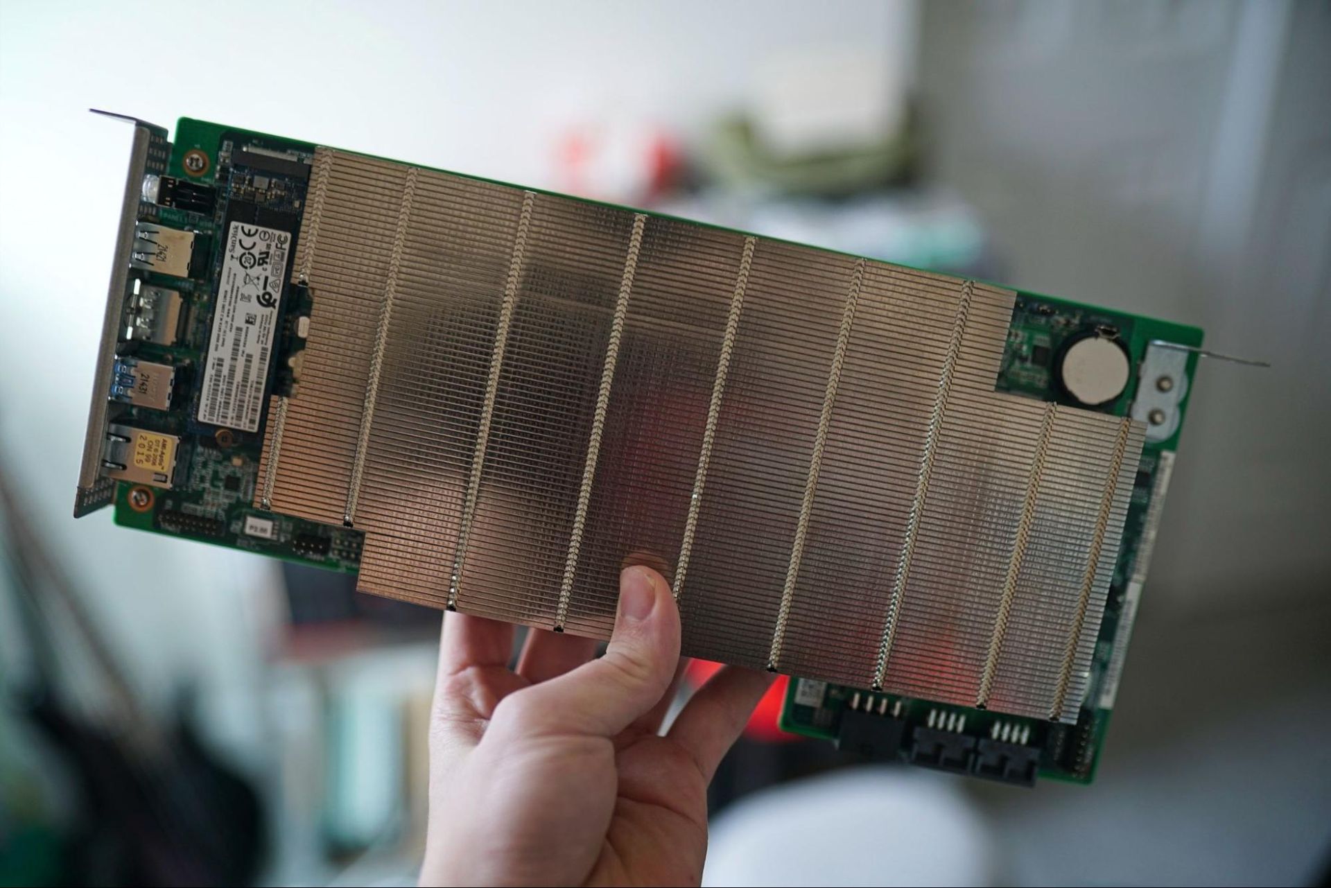
Modders have slashed the cost of running FSR 4 on AMD’s RDNA 2-powered BC-250 by nearly half, with a new implementation cutting the upscaler’s processing time from 11.51 ms to 5.92 ms at 1440p. Detailed in a VideoCardz post, the latest work builds on the community’s ongoing effort to turn AMD’s unusual PlayStation 5-derived crypto-mining board into a capable Linux gaming machine, while moving the FSR 4 optimizations from a custom Mesa modification into a portable FidelityFX DLL.
According to testing shared by the developer, FSR 4.1.1 running at 2560 x 1440 with a 1706 x 960 Quality input required 11.51 ms using the original shaders, compared with 5.92 ms using the latest v4.0.0-rc9 release. At 4K, processing time reportedly dropped from 25.72 ms to 12.08 ms, while 1080p fell from 7.13 ms to 3.93 ms. The developer also reports that the optimized implementation produced byte-identical images to the original shaders in controlled testing, suggesting that the performance improvement comes from executing the same workload more efficiently, and not reducing image quality.
The BC-250 is particularly interesting in this context because it is based on much older RDNA 2 graphics hardware. FSR 4 relies heavily on machine-learning workloads and accelerated low-precision integer operations that are far better suited to newer AMD architectures. On the BC-250, those operations have to be handled through alternative instruction paths.
Earlier community work tackled the problem in Mesa, optimizing the INT8 dot-product operations used by FSR 4. Instead of relying on a much more expensive fallback sequence, the modified implementation used a more efficient mathematical path based around signed 24-bit integer operations. One representative shader reportedly fell from 64,269 instructions to 37,613.
The latest fork takes that work a step further by shifting the optimizations into a FidelityFX DLL. This removes the requirement to run a specially modified Mesa build, potentially making the optimized path easier to use with an existing OptiScaler installation or games with compatible native FidelityFX implementations.
Native Windows support, other GPUs, and frame generation have not yet been qualified, as the developer tested the BC-250 on Linux using standard Mesa and GE-Proton. The practical upper target for the board is roughly 1440p, as FSR 4 still consumes 12.08 ms at 4K even after the optimization.
The achievement is the latest chapter in the BC-250's unusual story. ASRock built the board for cryptocurrency mining systems around PlayStation 5-class AMD silicon, with six Zen 2 CPU cores and 24 RDNA 2 compute units enabled by default. With the mining market's collapse, individual boards began filtering onto the second-hand market for well under $150, and enthusiasts have since assembled a mature Linux gaming ecosystem around them, complete with custom firmware, GPU governors, CU unlock tools, cases, cooling solutions, and distro-specific fixes.
The ecosystem still comes with limitations. In our testing, the BC-250’s aging Zen 2 CPU became a substantial bottleneck at 1080p and 1440p in some games, even with the GPU fully unlocked. The board also has only 16GB of shared GDDR6 memory, which caused some titles to crash due to memory issues at 4K and made frame generation harder at higher resolutions. While FSR 4 will not erase those limitations, halving the upscaler's per-frame cost gives a once-discarded mining board significantly more headroom to spend elsewhere.
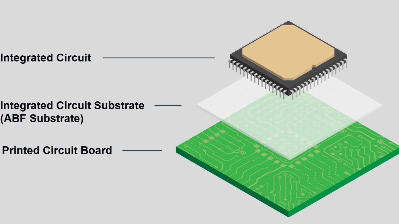
ABF substrates, the specialized insulating and wiring bases that connect tiny silicon chips above them to the much larger printed circuit boards below, sit beneath most high-end CPUs, GPUs, and AI accelerators. Featuring the Ajinomoto build-up film (ABF), these substrates have been critical to the semiconductor industry since the late 1990s, with personal computers, workstations, servers, and networking silicon driving steady demand for decades.
The artificial intelligence boom has multiplied that demand exponentially. Training and inference for frontier models now run across data centers, each housing hundreds of thousands of accelerators and providing hundreds of megawatts of compute. Nvidia alone shipped an estimated 3.2 million Blackwell GPU packages through the end of 2025, with every one of those accelerators packaged on an ABF substrate. Meanwhile, the industry is already entering the gigawatt era with humongous data center buildouts, each expected to house millions of AI accelerators.
This edifice rests on a remarkably narrow supply chain. Practically every advanced logic and AI chip made today by Intel, AMD, and Nvidia depends fundamentally on ABF substrates. These substrates are the conventional default for high-performance packaging. They are made by a small group of specialists, including Unimicron, Ibiden, Kinsus, Shinko Electric Industries, Samsung Electromechanics, and Nan Ya PCB. The upstream supply chain gets much tighter.
The one common denominator across ABF substrates, regardless of manufacturer, is the Ajinomoto build-up film itself. Each substrate maker laminates its build-up layers using dielectric film supplied by Japan's Ajinomoto, which controls a reported 95% or more of the global market. A single company, better known for food seasoning than microelectronics, sits at the base of one of the most concentrated supply chains in computing, almost singlehandedly supplying a material for hundreds of millions of semiconductor devices. Not surprisingly, demand is now growing beyond what the supply chain can comfortably supply.
Compounding this crunch, modern AI accelerators now pack multiple compute, memory, and supporting components onto a single board. As a result, the substrate is getting larger across the X-Y footprint to accommodate the expanding package. Manufacturers are also adding more build-up layers to the substrate to route the growing number of signals and power connections. Each additional layer requires another ABF layer, further multiplying demand across millions of accelerators and extending manufacturing times.
Unfortunately, the complications don't stop there. Beyond further straining the supply chain, expanding the substrates is creating technical problems, such as warpage, yield issues, and electrical losses within the component itself. This leaves the ABF substrate ecosystem facing two related challenges: producing enough advanced substrates for a rapidly expanding fleet of AI accelerators, while simultaneously re-engineering these substrates so they can continue to scale without becoming unmanufacturable or impractical.
The ABF substrate roadmap is consequently as much about supply-chain capacity as it is about the hardware itself, with suppliers such as Ajinomoto and Ibiden outlining plans to expand material and manufacturing capacity, respectively. At the same time, the wider industry — Intel, Samsung, and SK's Absolics among them — is exploring glass-core substrates and other material technologies to push past the limits of organic ABF.
ABF substrates
Silicon dies, including CPUs and GPUs, cannot communicate directly with the printed circuit board beneath them. The connection pads on a die are spaced micrometers apart, while the traces on a motherboard are spaced hundreds of micrometers to millimeters apart. Every high-performance chip, therefore, sits on an intermediary package substrate — a dense, multilayer board that fans the ultra-fine connections on the die outward into connections large enough for the motherboard to handle, while also providing signal routing, power and ground distribution, and mechanical support for the package.
ABF substrates used in AI accelerators typically consist of a rigid, glass-reinforced resin core sandwiched between successive build-up layers of copper wiring and insulating film. The core provides much of the mechanical rigidity, while the layers provide the increasingly dense wiring required close to the silicon.
To create the substrate, the manufacturer laminates the ABF dielectric onto the structure, forms microscopic vias — commonly with a CO2 laser — and then uses lithography and copper deposition to create a new wiring layer. High-end substrates typically use a semi-additive process (SAP), in which fine copper traces are plated up from a thin conductive seed layer. Another ABF layer is then laminated over it, and the process repeats. The film electrically separates successive copper layers, while plated microvias connect them vertically.
ABF substrate (Image credit: Ajinomoto)
Ajinomoto developed the film in the 1990s, after which it gradually became the industry default for its low dielectric loss, fine-line capability, and smooth lamination. The company reportedly accounts for roughly 95% of the substrate film market, with its nearest competitor, Sekisui Chemical, holding only a low-single-digit share.
The manufacturing tier above the film is more populated but still concentrated. Unimicron, Ibiden, and Shinko together account for roughly three-quarters of the substrate market by most estimates, with AT&S and Nan Ya PCB rounding out the leading group. These companies take ABF and other materials and manufacture the finished multilayer substrate. Semiconductor packaging companies, such as TSMC and Amkor, then integrate those substrates into packages containing the processor, memory, and other components.
AI accelerators are pushing substrates outward and upward
To deliver the compute and memory bandwidth that frontier models demand, the industry is packing ever more silicon onto each AI accelerator. Designers now place multiple large logic dies alongside a growing number of high-bandwidth memory stacks on a single package. Nvidia's Blackwell generation mounts two reticle-sized GPU dies and eight HBM3E stacks on a single package, with its upcoming Rubin and Rubin Ultra parts pushing it further still. TSMC's CoWoS packaging is scaling from around 3.3 reticles — each roughly 830 square millimeters of silicon — a generation ago to 5.5 reticles in volume production in 2026, with a roadmap reaching 9.5 reticles in 2027 and beyond 14 reticles by 2029, when a single package is expected to carry roughly ten compute dies and twenty or more memory stacks.
This expansion of the accelerator package is driving the substrate’s expansion on two physical levels. The first expansion is the substrate's footprint in the X-Y axes. The base has to get wider and longer to accommodate the larger package footprint. Ibiden's current roadmap puts its cutting-edge substrate size at 90 × 90mm (3.54 x 3.54 inches) in 2026, 110 × 110mm (4.33 x 4.33 inches) in 2028, and 130 × 130mm (5.12 x 5.12 inches) and larger from 2030 onward. Ajinomoto independently expects the representative advanced AI packages its film goes into to grow from roughly 100 mm² in 2026 to about 120 mm² for 3D AI packages from 2031.
The second expansion is along the Z axis through additional layers. An expanded collection of compute dies and memory creates more signals to route, while the corresponding increase in power draw requires extensive power and ground distribution, all of which must be carried in a growing number of layers. Ibiden's roadmap targets a 10-X-10 buildup structure in 2026, 12-X-12 in 2028, and 14-X-14 from 2030. Here, the numbers represent the build-up layers on either side of the central substrate core: “10-X-10” means 10 build-up layers per side of the core — which is represented by the “X” — each comprising one dielectric layer (ABF) plus one patterned copper layer, working as a pair.
Nan Ya PCB's roadmap points in the same direction. From an 11+N+11 baseline, it targets 24-layer substrates in 2026 and more than 24 layers in the first half of 2027, while tightening line and space from a 9/12 µm baseline to 8/8 µm and then to 6/7 µm by early 2027. Layer-counting conventions differ between vendors, so a per-side figure and a total layer count don't necessarily line up directly.
Nvidia's Blackwell architecture mounts two reticle-sized GPU dies and eight HBM3E stacks on a single package (Image credit: Nvidia)
The substrate’s expansion in both directions creates several challenges. Increasing the X-Y area makes the package harder to keep flat. Silicon, copper, the substrate core, and the polymer build-up materials that make up the substrate expand by different amounts when heated. As the package is bonded during assembly at around 250⁰C and then cooled, these mismatches cause the layers to pull against one another, leading to warping — a problem that becomes harder to control as package dimensions increase.
Excessive warpage can undermine solder-joint formation, layer-to-layer alignment, and reliability, while a larger substrate also occupies more manufacturing-panel area and exposes more area to potential defects. Organic substrates are reported to lose usable flatness once packages exceed roughly 120mm per side, a threshold that the largest AI accelerators are now reaching and that Ibiden's own roadmap — climbing toward 130mm and beyond — is set to cross.
The growing layer count along the z-axis also creates manufacturing challenges around yield, capacity, and time. Every new substrate layer requires a full manufacturing sequence of several steps, all held to sub-ten-micron tolerances. Each added layer increases the chance of a defect or alignment error that can scrap the whole substrate.
Additionally, layer count consumes manufacturing capacity and time in proportion. This is why Ibiden frames future demand in terms of semi-additive processing load rather than a simple substrate count, as a single advanced substrate now consumes far more of a line's capacity than a finished-unit tally would suggest.
Overall, the simultaneous expansion in substrate area and layer count means ABF consumption is rising much faster than processor shipments alone suggest. Ajinomoto illustrated this in its 2025 integrated report with a larger AI substrate that had about 3.5 times the board area and three times as many ABF layers as a conventional design — 18 layers against six — consuming roughly ten times as much ABF overall. This surging material consumption, set against an extremely concentrated supply base, extends the ABF substrate story beyond a technical problem into a supply-chain constraint.
The supply chain constraint
Like many components in the semiconductor industry chain before the AI boom, demand for ABF substrates periodically swung both ways. A severe bottleneck through 2020-2022 — driven by pandemic-era PC and server demand — was followed by an oversupply in 2023, as substrate manufacturers expanded capacity. However, that capacity was built for low-layer-count, smaller consumer substrates, not the large-body, multi-layer packages AI demands.
These advanced products require sufficiently large manufacturing formats, fine SAP wiring, tight layer registration, acceptable warpage, and high yields across much larger structures. Ibiden captures this by measuring demand not in finished substrates but in semi-additive-process load — the actual processing work each part imposes on a line. Indexing 2024 at 1.0, it expects the SAP load of a single AI-server substrate to reach 1.8 times that in 2026 and 2.5 times in 2028, with the company stating that substrate expansion will push total SAP demand beyond industry supply capacity, indicating a constraint in the manufacturing process itself.
The bottleneck is even tighter at the ABF material level. Ajinomoto's film capacity was already running at full load in the second quarter of 2026, at a reported two million square meters per month, although the company has outlined plans to increase capacity. A near-monopoly supplier at full capacity while consumption surges paints a clear picture of the bottleneck’s severity.
Unsurprisingly, prices have moved accordingly. Ajinomoto notified substrate manufacturers in May 2026 that it would raise ABF film prices by approximately 30%, effective in the third quarter. The hike is coming alongside comparable increases in copper-clad laminates from Resonac and Mitsubishi Gas Chemical, compounding pressure across the whole stack. Further tightening the squeeze, Ajinomoto recently cut shipments of the critical ABF film to China by 30%.
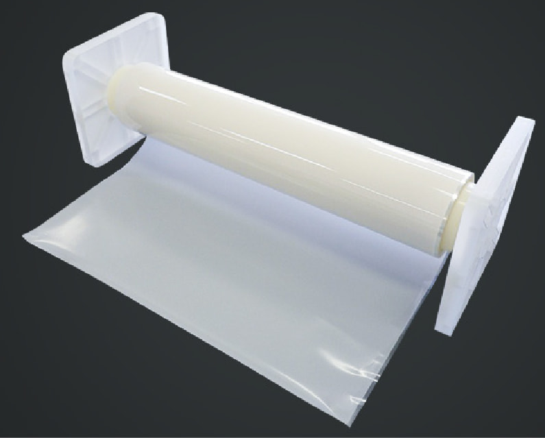
Ajinomoto Build-up film (Image credit: Ajinomoto)
The growing ABF substrate problem cannot simply be attributed to Ajinomoto running out of film. In fact, while it's running at full capacity, the company says it has no concerns about its overall supply chain. The constraint stretches across the entire chain containing ABF, glass cloth, and other materials, SAP equipment, large-format substrate factories, yield, and customer-qualified production capacity.
The immense industry demand is progressively tightening the crunch. Several supply-chain analyses converge on an ABF supply-demand shortfall of roughly 10% in the second half of 2026, widening to around 21% in 2027 and potentially exceeding 40% by 2028, with demand for substrate area projected to grow at a compound annual rate near 39% from 2025 to 2028 as accelerators integrate more components.
The roadmap to recovery: more capacity, better materials
The industry is responding to ABF substrates' multifaceted constraints on multiple fronts: expanding manufacturing capacity to relieve near-term supply pressure while qualifying new materials and substrate architectures to break through the technical limits. Capacity expansion is already underway across the supply chain.
Ibiden is executing ¥500 billion ($3.1 billion) in capital investment across fiscal years 2026 to 2028 — the largest single substrate expansion on record — targeting 2.8 times its 2024 capacity for ASIC and AI-server substrates by 2028. Unimicron raised its 2026 capital spending to a record NT$34 billion ($1.07 billion), with a focus on ABF substrates. Meanwhile, Samsung Electro-Mechanics, Samsung's substrate arm, has committed $1.2 billion to expand ABF substrate production, with volume production expected by the third quarter of 2027.
Pegatron's substrate unit, Kinsus, has approved NT$23.5 billion ($722 million) for ABF equipment over three years and now focuses its most advanced lines almost entirely on AI clients, aiming to lift monthly output at its Taoyuan plant by roughly 25% by 2027. While these projects address the shortage directly, their lead times mean the crunch may continue for a while, as supply cannot respond instantly to the AI demand spike.
Ajinomoto is expanding upstream as well. A new plant in Gunma entered full operation in 2025. The company has invested roughly ¥25 billion ($157 million) in ABF production since 2023 and has said it will invest at least as much again by 2030, targeting a capacity increase of more than 50%. It is also adding a third Japanese base for varnish production — envisioned to provide capacity comparable to Gunma — with construction planned for 2028 and operations to begin in 2032.
However, capacity only solves the problem if the current substrate architecture can continue to scale. The material roadmap — aimed at addressing the physical constraints of ABF substrates — is therefore advancing parallel to the factory roadmap. Ajinomoto says present and future ABF generations are being engineered for larger, more multilayered substrates, high-bandwidth I/O, lower transmission loss, and improved resistance to warpage and humidity. The company expects newer, higher-value ABF grades to take an increasing share of its portfolio through 2030.
Substrate makers are addressing the problem from the process side. Nan Ya plans to move beyond 150 mm body sizes and 24 layers while shrinking copper line/space geometry toward 6/7 microns in the first half of 2027. Its materials roadmap includes an ultra-low-CTE core material with a CTE below 3 ppm/°C, alongside low-Dk, low-Df, and low-CTE dielectrics. Finer wiring allows a substrate to support more connections without relying solely on additional area or layers, while low-expansion materials help keep the growing structure flat.
Eventually, the substrate's central core itself may change to glass. Organic substrate cores are increasingly difficult to keep dimensionally stable as packages approach and surpass 100 mm. Glass can be matched more closely to silicon's thermal expansion — providing dimensional stability — and offers substantially lower dielectric loss for high-speed links. It has therefore emerged as one of the industry's main solutions to warpage.
(Image credit: Intel)
As we detailed in our glass substrate roadmap, the move to a glass core is drawing a broad field, as it sits at the intersection of substrate-making, glass manufacturing, and advanced packaging, pulling in chip-and-packaging houses, display and glass specialists, and the incumbent substrate makers alike. Intel demonstrated a package that combines EMIB with a glass substrate at NEPCON Japan in January 2026, although the company still places commercial glass-substrate deployment in the latter half of the decade.
SK Group subsidiary Absolics is operating a low-volume glass-substrate manufacturing facility in Covington, Georgia — backed by $100 million in US CHIPS Act funding — producing prototype and qualification samples for customers, such as AMD for its MI400-series accelerators, while Samsung Electro-Mechanics is producing prototypes on a pilot line in Sejong and now plans mass production through its glass-core joint venture after 2027.
TSMC, meanwhile, is pursuing panel-level packaging through its chip-on-panel-on-substrate (CoPoS) platform, moving to a 310 x 310mm panel format, with a pilot line at its VisEra subsidiary, trial production targeted for 2027 and mass production for the second half of 2028. Glass-core substrates are a separate, later step on TSMC's roadmap, with commercial scale projected after 2030. Ibiden also puts “glass core” on its substrate technology roadmap around 2030 as a solution for warpage control.
The glass core — most likely a late-2020s-to-2030s technology — is positioned as a solution to the warpage wall. It replaces the organic core, not the ABF itself, which would remain the buildup material. A glass core may soften ABF demand per package, as glass's flatness allows finer routing and potentially fewer buildup layers, but it does not remove the material or the dependency. There's the possibility that a future dielectric material will eventually replace ABF, although that doesn't seem to be the industry's main focus currently.
Regardless, the near-term roadmap centers on more advanced SAP capacity, rapidly expanding factories, improved materials, and increased supply. Through the late 2020s, finer wiring, lower-loss ABF, lower-CTE materials, and better warpage control will enable organic substrates to stretch toward 110 mm and beyond. Around 2030, glass cores offer a path toward the 130 mm-plus packages that Ibiden and others already have on their roadmaps.
Sony Japan has officially implemented a new customer harassment policy to address ongoing customer backlash, following the company’s controversial announcement to phase out physical PlayStation game discs by January 2028. In an official publication on September 1, the company outlined prohibited customer behaviors to protect the dignity and safety of its employees and threatened to suspend customer service if the behaviors continued.
“The dignity and safety of our employees must not be threatened by customer harassment, such as words or demands from customers that exceed what is considered reasonable according to social norms,” the publication read. “If any behavior constituting customer harassment is confirmed, we may restrict or suspend customer service in order to protect the safety of our employees.”
Some of the examples of customer harassment detailed in the publication include “persistent and repeated, or prolonged, demands; excessive or unreasonable demands for compensation; abusive language, threats, slander, and other similar behaviors; requests unrelated to products or services; intimidating attitude; discriminatory or sexual conduct; and attacks and demands against individual employees.
The company also listed “forcing someone to prostrate themselves,” visiting company grounds without permission, and excessively asking for apologies as customer harassment, expressing willingness to use legal force if necessary. “We will take a firm stance against such actions and aim to build healthy and sustainable relationships while respecting both our customers and employees,” it said. “If we deem it necessary, we will cooperate with the police, lawyers, etc., and consider taking action, including legal measures and criminal proceedings.”
The new policies appear to be in response to the intense backlash over Sony's decision to end physical disc production by 2028. The decision was met with immediate, widespread backlash from the gaming community, which argued — among other things — that ending physical discs was equivalent to eliminating true ownership. Critics also argued that digital purchases were rentals and placed too much power in the company's hands, which could restrict access at will. Just 6 days after the July 1st announcement, a Change.org petition to stop the move had amassed 200,000 signatures and is now approaching 400,000.
The company doesn't appear to be backing down. After a class action lawsuit related to Sony’s decision to kill physical discs, the company moved to force the case into out-of-court arbitration, arguing that “reasonable consumers would not be misled into believing they own digital games.” The plaintiffs allege that Sony misleads consumers by using "Buy" buttons for digital PlayStation games without clearly disclosing that buyers are only purchasing a temporary, revocable license rather than actual, permanent ownership of the game.
Several other related lawsuits are ongoing. Regardless, Sony has said it will "cautiously move forward" with its decision despite “strong views” from players. The company hopes its new customer harassment policy will curb some of the backlash individual employees are currently facing. The policies also align with Japan's recent law that mandates companies to take measures to prevent customer harassment towards their workers.
Hackers reportedly claiming to be good actors have drained about $320 million worth of Bitcoin from Liquid Network's federation wallet, according to a CoinDesk report. In an X post on September 6, Liquid — a Bitcoin sidechain developed by blockchain infrastructure company Blockstream — confirmed that 4,000 BTC, roughly 95% of the entire wallet's balance, had been withdrawn.
Interestingly, the post referred to those behind the exploit as “purported white-hat hackers,” echoing the hackers’ own claim, after they self-identified as “whitehats” in a message embedded in a Bitcoin transaction. They also reportedly requested an audience with Liquid via the on-chain message, promising to return the money once the vulnerability that enabled the exploit is fixed.
“Please fix the bug first,” the on-chain message said. "The chain is under risk at latest commit right now. Make sure every node is patched. Then we will transfer the money back safely after confirming the fix.” Liquid responded on-chain with its security team's contact and has reportedly moved communications to an encrypted channel. Meanwhile, the platform said it has suspended transactions and warns of service disruptions as federation members work to restore service.
Launched in 2018, Liquid is a federated sidechain designed to move Bitcoin faster and more privately than the main chain. Users lock BTC on Bitcoin and receive an equivalent token, L-BTC, on Liquid, which settles blocks roughly every minute and finalizes in about two minutes. Rather than relying on miners, the network is secured by a federation of more than 80 exchanges, brokers, and other financial firms. The block signing and the multisig wallet holding the pegged-in Bitcoin are handled by 15 rotating functionaries that require 11 signatures to move funds.
The mechanics behind the exploit are also unusual, as nothing appears to have been stolen in the conventional sense. For example, in January, the Solana-based platform Step Finance lost roughly $40 million after attackers compromised devices belonging to its executive team, gaining access to the keys that guarded its treasury wallets. According to Liquid, the coins left through the Peg-out Authorization Key (PAK), belonging to SideSwap, a decentralized exchange built on the sidechain.
However, Liquid said that the key had not been compromised, nor had any others. SideSwap gave a matching account, stating a customer sent 4,000 L-BTC to its peg-out service at 14:05 UTC, the service processed the order as it would any other, and the Liquid Federation paid out 3,996 BTC to the customer's Bitcoin address twenty-three minutes later. According to SideSwap, its systems had no way of distinguishing those coins from any other L-BTC.
A 52-year-old Belgian-Chinese man has been arrested on suspicion of espionage for allegedly transferring specialized semiconductor intellectual property and trade secrets from Belgian chipmaker BelGaN, where he worked, to China. According to an AP News report citing details released by Belgium's federal prosecutor’s office on September 7, the Beijing-born Belgian resident was taken into custody on May 10 at a Brussels airport while attempting to board a flight to China.
The suspect — identified by Belgian media only as H.L. — previously held a senior research position at the now-defunct BelGaN, which specialized in gallium nitride (GaN) semiconductors. Investigators suspect he was concurrently leading a Chinese chip firm, GanKool, which was developing the exact same specialized gallium nitride chip technology as BelGaN. The company was established only a few months after H.L. joined BelGaN and was financed by a Chinese investment fund. The suspect now faces charges of industrial espionage, membership in a criminal organization, misuse of company assets, and unlawful disclosure of business secrets.
The espionage allegations emerged from an investigation into BelGaN's collapse. When the company collapsed into bankruptcy in the summer of 2024, Belgian authorities launched a routine financial probe into the failure. Investigators eventually uncovered highly unusual corporate activity. Instead of trying to keep BelGaN financially viable, the managers and the researcher may have actively tried to make the Belgian company “disappear” after transferring its proprietary knowledge. This led to further investigations that revealed GanKool’s existence and its connections to BelGaN.
In addition to the researcher’s role, the investigators also found evidence linking BelGaN's last CEO, a Chinese national, to the same Chinese rival. The prosecutors have said a second suspect remains at large, with Belgian media speculating that the CEO is the suspect.
The incident highlights the increasingly intense competition over technology and intellectual property in the semiconductor industry, particularly as China pushes to reduce its reliance on foreign chip technology while the U.S. continues to restrict its access to advanced processors and semiconductor manufacturing equipment. Just last month, South Korean court documents accused Chinese memory maker CXMT of using a detailed “Project Hefei” roadmap to obtain Samsung's proprietary DRAM technology, including a 620-step process recipe. A former Samsung engineer has already been sentenced to seven years in prison over the scheme.

 Login